
 100% FREE ACCESS
12th Standard Syllabus & Materials
12th Standard
TN 12th Computer Applications மின்னணு தரவு பரிமாற்றம் Sample Question Papers Study Material - QB365 Set A
NEW12th Standard
TN 12th Computer Applications மின் - வணிக பாதுகாப்பு அமைப்புகள் Sample Question Papers Study Material - QB365 Set A
NEW12th Standard
TN 12th Computer Applications மின்னணு செலுத்தல் முறைகள் Sample Question Papers Study Material - QB365 Set A
NEW12th Standard
TN 12th Computer Applications மின் - வணிகம் Sample Question Papers Study Material - QB365 Set A
NEW12th Standard
TN 12th Computer Applications திறந்த மூல கருத்துருக்கள் Sample Question Papers Study Material - QB365 Set A
NEW12th Standard
TN 12th Computer Applications வலையமைப்பு வடமிடல் Sample Question Papers Study Material - QB365 Set A

Published on: 02/01/2020
Semiconductor Electronics
Download Tamil Nadu 12th Standard Physics question papers, model tests, one-mark questions, important questions, and public exam papers in PDF format. Free study materials and answer keys for TN State Board students.
Questions + Answers key
Take MCQ Physics Test1.
By adding _________ impurity in intrinsic semi conductor, p type semiconductor is made. Charge of these p type semiconductor is ____________
Trivalent, neutral
Pentaralent, neutral
Pentavalent, positive
Trivalent, negative
2.
C, Si and Ge have same no of valence electrons. C is an insulator because energy required to take one electron out from ______________.
Si is more
C is more
Ge is more
C is less
3.
A forward biased diode is treated as ________________.
An open switch with infinite resistance
A closed switch with a voltage drop of 0V
A closed switch in series with a battery voltage of 0.7V
A closed switch in series with a small resistance and a battery
4.
If a small amount of antimony (Sb) is added to germanium crystal,______.
it becomes a p-type semiconductor
the antimony becomes an acceptor atom
there will be more free electrons than hole in the semiconductor
its resistance is increased
5.
Define energy band
6.
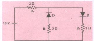
The given circuit has two ideal diodes connected as shown in figure below. Calculate the current flowing through the resistance R1.
7.
8.
Define electron motion in a semiconductor.
9.
For a BJT circuit shown, assume that the 'β' of the transistor is very large and VBE= 0.7 V. The mode of operation.
10.
Draw the circuit diagram of a half-wave rectifier and explain its working.
11.
Explain the formation of depletion region and barrier potential in PN junction diode.
12.
Elucidate the formation of a N -type and P-type semiconductors.
13.
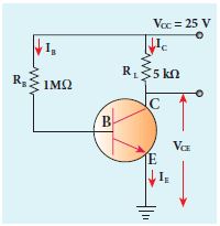
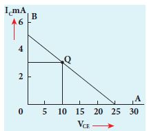
The current gain of a common emitter transistor circuit shown in figure is 120. Draw the DC load line and mark the Q point on it. (VBE to be ignored).
14.
| (a) | ENIAC | World's first computer |
| (b) | Energy levels | Electron volts |
| (c) | Bipolar junction | Bardeen |
| (d) | Reverse saturation current | IR |
15.
Assertion: Base current (IB) decreases and in turn increases the collector current.
Reason: Input signal (VS) decreases the forward voltage across the emitter-base.
Codes:
(a) Assertion and Reason are correct and Reason is the correct explanation of Assertion.
(b) Assertion and Reason are true but Reason is the false explanation of the Assertion.
(c) Assertion is true but Reason is false.
(d) Assertion is false but Reason is true.
16.
Incorrect statements
(a) A and B are inputs and Y is the output for OR gate.
(b) A is the input and Y is the output for NOT gate.
(c) A and B are outputs and Y is the input for NOR gate.
(d) A and B are inputs and Y is the output for Ex-OR gate.
17.
Correct Statement
(I) Transistor can be operated efficiently in an operating point
(II) Variations of Ic and VCE takes place in this point.
(III) Q - points determine the working point of a transistor.
(IV) Transistor is a semiconductor device used to amplify or switch electronic signals.
(a) I and II only
(b) II and III only
(c) I, II and III only
(d) I, II, III and IV only
1.
(a)
Trivalent, neutral
2.
(b)
C is more
3.
(d)
A closed switch in series with a small resistance and a battery
4.
(c)
there will be more free electrons than hole in the semiconductor
5.
Band of very large number of closely spaced energy levels in a very small energy range is known as energy band.
6.
V= 10V, R1 = 2 Ω, R3 = 2 Ω
Diode D1 is reverse biased so it will block the current and diode D2 is forward biased, so it will pass the current.
\(\mathrm{R} =\mathrm{R}_{1}+\mathrm{R}_{2} \)
\(=2+2=4 \Omega \)
\(\mathrm{I} =\frac{\mathrm{V}}{\mathrm{R}}=\frac{10}{4} \)
I = 2.5 A
7.
8.
(i) To move the hole in a given direction, the valence electrons move in the opposite direction.
(ii) Electrons flow in a N-type semiconductor is similar to electrons moving in a metallic wire.
(iii) The N- type dopant atoms will yield electrons available for conduction.
9.
VBE =0.7V
Input junction is a forward biased.
Since,
VBE = 0.7V
VCE = VBE+ VCB
VCB = VCE-VBE
To determine VCB we find IC
\({ I }_{ C }\cong { I }_{ C }\frac { 2-{ V }_{ BE } }{ { R }_{ 2 } } =\frac { 2-0.7 }{ 1k\Omega } \)
IC = 1.3mA
VCE = VCC - IC (R1 + R2)
= 10 - 1.3mA (10K + 1K)
VCE = - 4.3 V
VCE =-4.3V-0.7
VCB = - 5V
10.
HaIf wave rectifier:
Only one half of the input wave reaches the output. Therefore it is called half wave rectifier.
Construction:
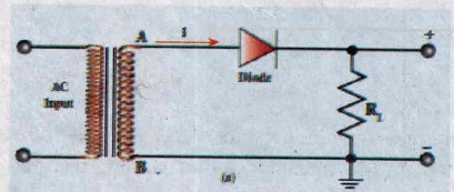
(i) The circuit consists of a transformer, a p-n junction diode and a resistor
(ii) In a half wave rectifier circuit, either a positive half or the negative half of the AC input is passed through by the diode while the other half is blocked
(iii) It acts as a rectifier diode.
.jpg)
(iv) Efficiency (η) is the ratio of the output DC power to the AC input power circuit. supplied to the circuit.
(v) The efficiency (η) of a half wave rectifier is found to be 40.6 %.
.jpg)
11.
i) Formation of depletion layer
(i) A single piece of semiconductor crystal is suitably doped such that its one side is p-type semiconductor and the other side is n-type semiconductor.
(ii) The contact surface between the two sides is called p-n junction. Whenever p-n junction is formed, some of the free electrons diffuse from the n-side to the p-side while the holes from the P-Side to the n-side.
(iii) The diffusion of charge carriers happens due to the fact that the n-side has higher electron concentration and the p-side has higher hole concentration.
(iv) The diffusion of the majority charge carriers across the junction gives rise to an electric current, called diffusion current.
(v) When an electron leaves the n-side, a pentavalent atom in the n-side becomes a positive ion.
(vi) The free electron migrating into p-side recombines with a hole present in a trivalent atom near the junction and the trivalent atom becomes a negative ion. Since such ions are bonded to the neighbouring atoms in the crystal lattice, they are unable to move.
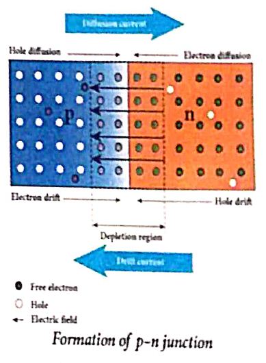
(vii) As the diffusion process continues, a laver of positive ions and a layer of negative ions are created on either side of the junction accordingly.
(viii) The thin region near the junction which is free from charge carriers (free electrons and holes) is called depletion region.
(ix) An electric field is set up between the positively charged layer in the n-side and the negatively charged layer in the p-side in the depletion region.
(x) This electric field makes electrons in the p-side drift into the n-side and the holes in the n-side into the p-side.
(xi) The electric current produced due to the motion of the minority charge carriers by the electric field is known as drift current. The diffusion current and drift current flow in opposite directions.
(xii) Though drift current is less than diffusion current initially, equilibrium is reached between them at a particular time.
(xiii) With each electron (or hole) diffusing across the junction, the strength of the electric field increases thereby increasing the drift current till the two currents become equal
(xiv)Hence at equilibrium, there is no net electric current across the junction. Thus, a p-n junction is formed.
ii) Junction potential or barrier potential
.JPG)
(i) The movement of charge carriers across the junction takes place only to a certain point beyond which the depletion layer acts like a barrier to further diffusion of free charges across the junction.
(ii) This is due to the fact that the immobile ions on both sides establish an electric potential difference across the junction.
(iii) Therefore, an electron trying to diffuse into the interior of the depletion region encounters a wall of negative ions repelling it backwards.
(iv) If the free electron has enough energy, it can break through the wall and enter into the p-region, where it can recombine with a hole and create another negative ion.
(v) The strength of the electric potential difference across the depletion region keeps on increasing with the crossing of each electron until equilibrium is reached, at this point, the internal repulsion of the depletion layer stops further diffusion of free electrons across the junction.
(vi) The difference in potential across the depletion layer is called the barrier potential (Vb).
(vii) At 25°C, this barrier potential is approximately 0.7 V for silicon and 0.3 V for germanium.
12.
n-type semiconductor:
(i) A n-type semiconductor is obtained by doping a pure Germanium (or Silicon) crystal with a dopant from group V pentavalent elements like Phosphorus, Arsenic, and Antimony.
(ii) The dopant has five valence electrons while the Germanium atom has four valence electrons.
(iii) During the process of doping, a few of the Germanium atoms are replaced by the group V dopants.
(iv) Four of the five valence electrons of the impurity atom are bound with the 4 valence electrons of the neighbouring replaced Germanium atom
(v) The fifth valence electron of the impurity atom will be loosely attached with the nucleus as it has not formed the covalent bond.
(vi) The energy level of the loosely attached fifth electron from the dopant is found just below the conduction band edge and is called the donor energy level.
(vii) At room temperature, these electrons can easily move to the conduction band with the absorption of thermal energy
(viii) Besides, an external electric field also can set free the loosely bound electrons and lead to conduction.
(ix) It is important to note that the energy required for an electron to jump from the valence band to the conduction band (Ee ) g in an intrinsic semiconductor is 0.7 eV for Ge and 1.1 eV for Si, while the energy required to set free a donor electron is only 0.01 eV for Ge and 0.05 eV for Si.
(x) The group V pentavalent impurity atorns. donate electrons to the conduction band and are called donor impurities. Therefore, each impurity atom provides one extra electron to the conduction band in addition to the thermally generated electrons.
(xi) These electrons leave holes in the valence band. Hence, the majority carriers of current in an n-type semiconductor are electrons and the minority carriers are holes. Such a semiconductor doped with a pentavalent impurity is called an n-type semiconductor.
p-type semiconductor:
(i) A trivalent atom from group III elements such as Boron, Aluminium, Gallium and Indium is added to the Germanium or Silicon substrate. The dopant with three valence electrons is bound with the neighbouring Germanium atom.
(ii) As Germanium atom has four valence electrons, one electron position of the dopant in the Germanium crystal lattice will remain vacant. The missing electron position in the covalent bond is denoted as a hole.
(iii) To make complete covalent bonding with all four neighbouring atoms, the dopant is in need of one more electron
(iv) These dopants can accept electrons from the neighbouring atoms. Therefore, this impurity is called an acceptor impurity The energy level of the hole created by each impurity atom is just above the valence band and is called the acceptor energy level band and is called the acceptor energy level.
(v) For each acceptor atom, there will be a hole in the valence band in addition to the thermally generated holes. In such an extrinsic semiconductor, holes are the majority carriers and thermally generated electrons are minority carriers. The semiconductor thus formed is called a p-type semiconductor.
13.
β = 120
Base current, \({ I }_{ B }=\frac { 25V }{ 1M\Omega } =\frac { 25 }{ 1\times { 10 }^{ 6 } } =25\mu A\)
We know that
\(\beta =\frac { { I }_{ C } }{ { I }_{ B } } \) (or)
IC = β IB = 120 x 25 μA
= 3000 μA = 3 mA
VCE = VCC - ICRC
= 25 - (3 mA x 5k) = 10 V
14.
(d) Reverse saturation current - IR
15.
(a) Assertion and Reason are correct and Reason is the correct explanation of Assertion.
16.
(c) A and B are outputs and Y is the input for NOR gate.
17.
(d) I, II, III and IV only

12th Standard Syllabus & Materials
12th Standard
TN 12th Computer Applications களப்பெயர் முறைமை (DNS) Sample Question Papers Study Material - QB365 Set A
NEW12th Standard
TN 12th Computer Applications வலையமைப்பு எடுத்துக்காட்டுகள் மற்றும் நெறிமுறைகள் Sample Question Papers Study Material - QB365 Set A
NEW12th Standard
TN 12th Computer Applications கணினி வலையமைப்பு ஓர் அறிமுகம் Sample Question Papers Study Material - QB365 Set A
NEW12th Standard
TN 12th Computer Applications PHP-உடன் MySQL-ஐ இணைத்தல் Sample Question Papers Study Material - QB365 Set A



Tamilnadu Stateboard 12th Standard Subjects

Maths

Chemistry
Physics

Biology

Computer Science

Business Maths and Statistics

Economics

Commerce

Accountancy

History

Computer Applications
Biology
Computer Technology
Computer Applications
Computer Science
Business Maths and Statistics
Commerce
Economics
Maths
Chemistry
Physics
Computer Technology
History
Accountancy

Tamil

English

French
Tamilnadu Stateboard Standards

