
 100% FREE ACCESS
12th Standard Syllabus & Materials
12th Standard
TN 12th Computer Applications மின்னணு தரவு பரிமாற்றம் Sample Question Papers Study Material - QB365 Set A
NEW12th Standard
TN 12th Computer Applications மின் - வணிக பாதுகாப்பு அமைப்புகள் Sample Question Papers Study Material - QB365 Set A
NEW12th Standard
TN 12th Computer Applications மின்னணு செலுத்தல் முறைகள் Sample Question Papers Study Material - QB365 Set A
NEW12th Standard
TN 12th Computer Applications மின் - வணிகம் Sample Question Papers Study Material - QB365 Set A
NEW12th Standard
TN 12th Computer Applications திறந்த மூல கருத்துருக்கள் Sample Question Papers Study Material - QB365 Set A
NEW12th Standard
TN 12th Computer Applications வலையமைப்பு வடமிடல் Sample Question Papers Study Material - QB365 Set A

Published on: 02/09/2022
QB365 provides a detailed and simple solution for every Possible Book Back Questions in Class 12 Physics Subject - Retirement and Death of a Partner, English Medium. It will help Students to get more practice questions, Students can Practice these question papers in addition to score best marks.
Download Tamil Nadu 12th Standard Physics question papers, model tests, one-mark questions, important questions, and public exam papers in PDF format. Free study materials and answer keys for TN State Board students.
Questions + Answers key
Take MCQ Physics Test1.
Assuming V CEsat = 0.2 V and \(\beta\) = 50, find the minimum base current (IB) required to drive the transistor given in the figure to saturation.
2.
Calculate the range of the variable capacitor that is to be used in a tuned-collector oscillator which has a fixed inductance of 150 μH. The frequency band is from 500 kHz to 1500 kHz.
3.
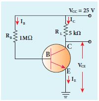
The current gain of a common emitter transistor circuit shown in figure is 120. Draw the DC load line and mark the Q point on it. (VBE to be ignored).
4.
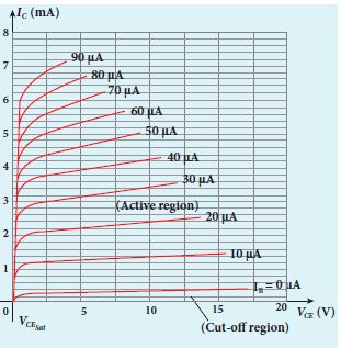
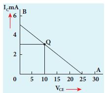
The output characteristics of a transistor connected in common emitter mode is shown in the figure. Determine the value of IC when VCE = 15 V. Also determine the value of IC when VCE is changed to 10 V
5.
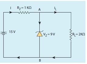
Find the current through the Zener diode when the load resistance is 2 kΩ. Use diode approximation.
6.
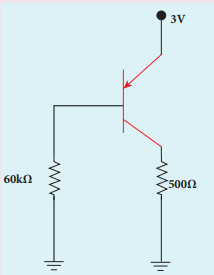
In the circuit shown in the figure, the BJT has a current gain (β) of 50. For an emitter-base voltage VEB = 600 mV, calculate the emitter-collector voltage VEC (in volts).
7.
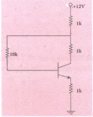
A transistor having α = 0.99 and VBE = 0.7V, is connected in the common-cmiitter configuration as shown in figure. If the transister is in saturation region, find the value of the collector current.
8.
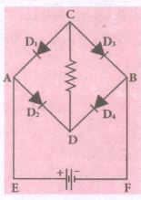
Four silicon diodes and a 10 Ω resistor are connected as shown in figure below. Each diode has a resistance of 1Ω. Find the current flows through the 10Ω resistor.
9.
Write a note on photodiode.
10.
Discuss the biasing polarities in an NPN and PNP transistors
11.
How electron-hole pairs are created in a semiconductor material?
12.
What do you mean by Internet of Things?
13.
Distinguish between wireline and wireless communication? Specify the range of electromagnetic waves in which it is used.
14.
Distinguish between avalanche breakdown and Zener breakdown.
15.
16.
State and prove De Morgan’s first and second theorem.
1.
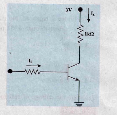
VCE sat = 0.2 V ; β = 50
Applying Kirchhoff's voltage law we get
\( \mathrm{V}_{\mathrm{CC}}=\mathrm{I}_{\mathrm{C}} \mathrm{R}_{\mathrm{C}}+\mathrm{V}_{\mathrm{CE sat}}=0 \)
(or)
\(I C=\frac{V_{C C}-V_{C Esat}}{R_{C}}=\frac{3-0.2}{10^{3}} =2.8 mA\)
\(I_B=\frac{I_C}{\beta}=\frac{2.8 mA}{50}=56 \mu A\)
2.
Resonant frequency, \({ f }=\frac { 1 }{ 2\pi \sqrt { LC } } \)
On simplifying, we get C = \(\frac { 1 }{ { 4\pi }^{ 2 }{ { f }^{ 2 } }L } \)
i) When frequency = 500 kHz,
\(C=\frac { 1 }{ 4\times { 3.14 }^{ 2 }\times { (500\times { 10 }^{ 3 }) }^{ 2 }\times 150\times { 10 }^{ -6 } } \)
= 676 pF
ii) When frequency = 1500 kHz,
\(C=\frac { 1 }{ 4\times { 3.14 }^{ 2 }\times { (1500\times { 10 }^{ 3 }) }^{ 2 }\times 150\times { 10 }^{ -6 } } \)
= 75 pF
Therefore, the capacitor range is 75 to 676 pF.
3.
β = 120
Base current, \({ I }_{ B }=\frac { 25V }{ 1M\Omega } =\frac { 25 }{ 1\times { 10 }^{ 6 } } =25\mu A\)
We know that
\(\beta =\frac { { I }_{ C } }{ { I }_{ B } } \) (or)
IC = β IB = 120 x 25 μA
= 3000 μA = 3 mA
VCE = VCC - ICRC
= 25 - (3 mA x 5k) = 10 V
4.
When VCE = 15 V, IC = 1.5 μA
When VCE is changed to 10 V, IC = 1.4 μA
5.
Voltage across AB, is VZ = 9V
Voltage drop across Rs = 15 - 9 = 6V
Therefore current through the resistor Rs,
I = \(\frac { 6 }{ 1\times { 10 }^{ 3 } } \) = 6 mA
Voltage across the load resistor, = VAB = 9V
Current through load resistor,
\({ I }_{ L }=\frac { { V }_{ AB } }{ { R }_{ L } } =\frac { 9 }{ 2\times { 10 }^{ 3 } } =4.5mA\)
The current through the Zener diode,
IZ = I - IL = 6 mA - 4.5mA = 1.5 mA
6.
\(\beta =50 \)
\(V_{\beta E} =600 \mathrm{mV} \)
\(=0.6 \mathrm{~V} \)
\(\mathrm{V}_{\mathrm{B}} =\mathrm{V}_{\mathrm{E}}-\mathrm{V}_{\mathrm{EB}} \)
\(\mathrm{V}_{\mathrm{B}} =3-0.6 \)
\(=2.4 \mathrm{~V} \)
\(\mathrm{I}_{\mathrm{B}} =\frac{\mathrm{V}_{\mathrm{B}}}{R_B}=\frac{2.4}{60 \times 10^3}=40 \mu \mathrm{A} \)
\(\mathrm{I}_{\mathrm{C}} =\beta \mathrm{I}_{\mathrm{B}}=50 \times 40 \mu \mathrm{A} =2 \mathrm{~mA} \)
\(V_C=R_FI_C=500 \times 2 \times10^{-3}=1 V\)
\(V_{EC}=V_E-V_C\)
\(V_{EC}=V_E-V_C\)
\(V_{EC}=3-1=2V\)
7.
\(\mathrm{V}_{\mathrm{cc}}=12 \mathrm{~V}, \mathrm{R}_{\mathrm{B}}=10 \mathrm{k} \Omega, \mathrm{R}_{\mathrm{E}}=1 \mathrm{k} \Omega, \mathrm{R}_{\mathrm{c}}=1+1=2 \mathrm{k} \Omega, \alpha=0.99, \mathrm{~V}_{\mathrm{BE}}=0.7 \mathrm{~V}, \mathrm{I}_{\mathrm{c}}=?\)
\(\beta=\alpha /(1-\alpha)=0.99 /(1-0.99)=99\)
\(\mathrm{I}_{\mathrm{B}}=\mathrm{I}_{\mathrm{C}} / \beta=\mathrm{I}_{\mathrm{c}} / 99\)
Applying Kirchoff's Voltage law,
\(I_C R_C+I_n R_n+I_E R_E+V_{u t}=V\)
\(2 \times 10^3 \mathrm{I}_{\mathrm{C}}+10 \times 10^3\left(\mathrm{I}_{\mathrm{C}} / 99\right)+1 \times 10^3\left(\mathrm{I}_{\mathrm{C}}+\mathrm{I}_{\mathrm{C}} / 99\right)+0.7=12 \quad\left(\because \mathrm{I}_{\mathrm{E}}=\mathrm{I}_{\mathrm{n}}+\mathrm{I}_{\mathrm{C}}\right)\)
\(\therefore \mathrm{I}_{\mathrm{C}}=\frac{11.3 \times 10^{-3} \times 99}{298}\)
\(\mathrm{I}_{\mathrm{C}}=3.7 \times 10^{-3} \mathrm{~A}=3.7 \mathrm{~mA}\)
8.
Diode D1 and D4 is reverse biased [open]
Diode D1 and D3 are forward biased.
The resistances are in series
R = 1 + 10 + 1 - 12 Ω
Barier Potential, V = 0.7 + 0.7 = 1.4 V (Silicon diode)
Applying Kirchhoff's voltage Law,
0.7 + I(1) + I(10) + 0.7 + I(1) = 3V
12 I = 3 - 1.4
12 I = 1.6
\(I=\frac{1.6}{12}=\mathbf{0 . 1 3 3 A}\)
9.
Photo diode:
A p -n junction diode which converts an optical signal into electrical current is known as photodiode.
(i) The operation of photodiode is exactly inverse to that of an LED. Photodiode works in reverse bias condition.
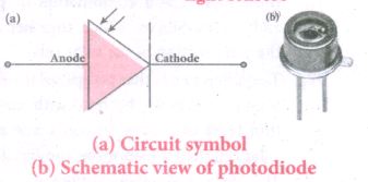
(ii) The direction of arrows indicates that the light is incident on the photo diode.
(iii) The device consists of a p-n junction semiconductor made of photosensitive material kept safely inside a plastic case as shown in fig.
(iv) It has a small transparent window that allows light to be incident on the p-n junction.
(v) Photodiodes car generate current when the p - n junction is exposed to light and hence are called as light sensors.
(vi) When a photon of sufficient energy (hv) strikes the depletion region of the diode, some of the valence band electron are elevated into conduction band, in turn holes are developed in the valence band. This creates electron-hole pairs. The amount of electron - hole pairs generated depends on the intensity of light incident on the p - n junction.
(vii) These electron and holes are swept across the p-n junction by the electric field created by reverse voltage before recombination takes place. Thus, holes move towards the n - side and electrons towards the P - side - when the external circuit is made, the electrons flow through the external circuit and constitute the photo current.
(viii) When the incident light is zero, there exists a reverse current which is negligible. This reverse current in the absence of any. incident light is called dark current and is. due to the thermally generated minority carriers.
10.
(i) In NPN transistor, a positive voltage is given to the collector terminal to produce a current flow from the collector to the emitter.
(ii) In a PNP transistor, a positive voltage is given to the emitter terminal to produce current flow from the emitter to collector.
(iii) To operate the transistor in the active region, emitter-base must be forward biased and collector base must be reverse biased.
11.
(i) A Semiconductor in its pure form without impurity is called an intrinsic semiconductor.
(ii) Impurity means any other atom in the crystal lattice.
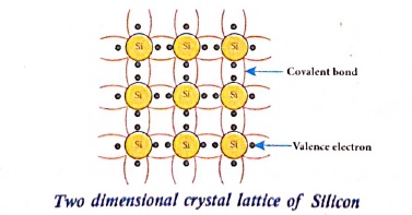
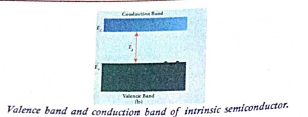
(iii) Each silicon atom has four electrons in the outmost orbit and is covalently bonded with the neighboring atoms to form the lattice. The band diagram is shown in the figure.
(iv) A small increase in temperature is sufficient enough to break some of the covalent bonds and release the electrons free from the lattices as shown in figure.
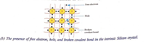
(v) The vacancies produced in the valence band are called holes. As the holes are dericiency of electrons, they are treated to possess positive charges Hence electrons and holes are the two charge carriers in semiconductors.
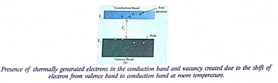
(vi) The number of electrons in the conduction band is equal to the number of holes in the valance band. The conduction is done to the electrons in the conduction band and holes in the valence band.
\(\begin{array}{l}
I=I_c+I_{\mathrm{h}} \\
I=\text { Total current } \\
I_e=\text { Electron current } \\
I_{\mathrm{h}}=\text { hole current }
\end{array}\)
(vii) It behaves like an insulator at 0 K. The increase in temperature increases the number of charge carriers.
(viii) The intrinsic carrier concentration is the number of electron in the conduction band or number of holes in the valence band in an intrinsic semi conductor.
12.
i) Internet is a fast-growing technology in the field of a communication system with multifaceted tools.
ii) It provides new ways and means to interact and connect with people.
iii) Internet is the largest computer network recognized globally that connects millions of people through computers.
iv) It finds extensive applications in all walks of life.
13.
| Wireline | Wireless |
|---|---|
| Wireline communication (point-point communication) uses mediums like wires, cables, and optical fibers. | Wireless communication uses free space as a communication medium. |
| These systems cannot be used for long-distance transmission they are connected physically. | The signals are transmitted in the form of electromagnetic waves with the help of a transmitting antenna Hence wireless communication is used for long-distance transmission |
| Examples are telephone, intercom, and cable TV. | Examples are mobile, radio or TV broadcasting, and satellite communication. |
| Wireline up to 100 meters | Wireless up to several thousand kilometers |
It is the maximum distance between the source and the destination up to which the signal is received with sufficient strength.
14.
| S.No | Avalanche breakdown | Zener breakdown |
| (i) | Heavily doped p-n junctions have narrow depletion layers of the order of <10-6 m. | It occurs in lightly doped junctions Which have wide depletion layers. |
| (ii) | Electric field produced is strong in nature. | Weak electric field is produced. |
| (iii) | When a reverse voltage across the junction is increased to the breakdown limit, a very strong electric field is set up. It ruptures the covalent bonds in the lattice and thereby generating electronic-hole pairs. This effect is called Zener effect | Thermally generated minority charge carriers accelerated by the electric field gains sufficient kinetic energy, collide with the semiconductor atoms while passing through the depletion region. This leads to the breaking of covalent bonds and in turn covalent bonds and in turn generates electron-hole pairs |
| (iv) | Even a small further increases in reverse voltage produces a large number of charge carriers. Hence the junction has very low resistance in the breakdown region. | The newly generated charged carriers are also accelerated by the electric field resulting in more collisions and further production of charged carriers. |
| (v) | This process of emission of electrons due to the strong electric field is known as internal field emission or field ionization. | This cumulative process leads to an avalanche of charge carriers across the junction and consequently reduces the reverse resistance the diode current increases sharply. |
15.
16.
First Theorem :
The complement of the sum of two logical inputs is equal to the product of its complements.
\(\overline { A+B } \) = \(\bar { A } .\bar { B } \)
Proof:
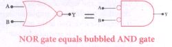
(i) The Boolean equation for NOR gate is Y = \(\overline { A+B } \)
(ii) The Boolean equation for a bubbled AND gate is Y =\(\bar { A } .\bar { B } \)
(iii) Both cases generate same outputs for same inputs. It can be verified using the following truth
| A | B | A+B | \(\overline { A+B } \) | Ā | \(\bar { B } \) | \(\bar { A } .\bar { B } \) |
| 0 | 0 | 0 | 1 | 1 | 1 | 1 |
| 0 | 1 | 1 | 0 | 1 | 0 | 0 |
| 1 | 0 | 1 | 0 | 1 | 0 | 0 |
| 1 | 1 | 1 | 0 | 0 | 0 | 0 |
(i) From the above truth table, we can conclude \(\overline { A+B } \) = \(\bar { A } .\bar { B } \)
(ii) Thus De Morgan's first theorem is proved.
(iii) Hence, a NOR gate is equal to a bubbled AND gate
Second theorem :
The complement of the product of two is equal to the sum of its complements
\(\overline { A.B } \) = \(\bar { A } +\bar { B } \)
Proof:
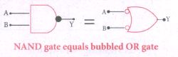
(i) The Boolean equation for NAND gate is Y = \(\overline { A.B } \)
(ii) The Boolean equation for bubbled OR gate is Y = \(\bar { A } +\bar { B } \)
(iii) A and B are the inputs and Y is the output. The above two equations produces the same output for the same inputs. It can be verified by using the truth table.
| A | B | A+B | \(\overline{\mathrm{A}. \mathrm{B}}\) | Ā | \(\bar { B } \) | \(\overline{\mathrm{A}}+\overline{\mathrm{B}}\) |
| 0 | 0 | 0 | 1 | 1 | 1 | 1 |
| 0 | 1 | 0 | 1 | 1 | 0 | 1 |
| 1 | 0 | 0 | 1 | 0 | 1 | 1 |
| 1 | 1 | 1 | 0 | 0 | 0 | 0 |
(i) From the above truth table, we can conclude \(\overline { A.B } \) = \(\bar { A } +\bar { B } \)
(ii) Thus, De Morgan's second therom is proved.
(iii) Hence, a NAND gate is equal to a bubbled OR gate.

12th Standard Syllabus & Materials
12th Standard
TN 12th Computer Applications களப்பெயர் முறைமை (DNS) Sample Question Papers Study Material - QB365 Set A
NEW12th Standard
TN 12th Computer Applications வலையமைப்பு எடுத்துக்காட்டுகள் மற்றும் நெறிமுறைகள் Sample Question Papers Study Material - QB365 Set A
NEW12th Standard
TN 12th Computer Applications கணினி வலையமைப்பு ஓர் அறிமுகம் Sample Question Papers Study Material - QB365 Set A
NEW12th Standard
TN 12th Computer Applications PHP-உடன் MySQL-ஐ இணைத்தல் Sample Question Papers Study Material - QB365 Set A



Tamilnadu Stateboard 12th Standard Subjects

Maths

Chemistry
Physics

Biology

Computer Science

Business Maths and Statistics

Economics

Commerce

Accountancy

History

Computer Applications
Biology
Computer Technology
Computer Applications
Computer Science
Business Maths and Statistics
Commerce
Economics
Maths
Chemistry
Physics
Computer Technology
History
Accountancy

Tamil

English

French
Tamilnadu Stateboard Standards

