
 100% FREE ACCESS
12th Standard Syllabus & Materials
12th Standard
TN 12th Computer Applications மின்னணு தரவு பரிமாற்றம் Sample Question Papers Study Material - QB365 Set A
NEW12th Standard
TN 12th Computer Applications மின் - வணிக பாதுகாப்பு அமைப்புகள் Sample Question Papers Study Material - QB365 Set A
NEW12th Standard
TN 12th Computer Applications மின்னணு செலுத்தல் முறைகள் Sample Question Papers Study Material - QB365 Set A
NEW12th Standard
TN 12th Computer Applications மின் - வணிகம் Sample Question Papers Study Material - QB365 Set A
NEW12th Standard
TN 12th Computer Applications திறந்த மூல கருத்துருக்கள் Sample Question Papers Study Material - QB365 Set A
NEW12th Standard
TN 12th Computer Applications வலையமைப்பு வடமிடல் Sample Question Papers Study Material - QB365 Set A

Published on: 03/12/2019
Semiconductor Electronics
Download Tamil Nadu 12th Standard Physics question papers, model tests, one-mark questions, important questions, and public exam papers in PDF format. Free study materials and answer keys for TN State Board students.
Questions + Answers key
Take MCQ Physics Test1.
The intrinsic semi-conductor has ______________.
A finite resistance which does not change with temperature
Infinite resistance which decreases with temperature
Finite resistance which decreases with temperature
Finite resistance which does not change with temperature
2.
By adding _________ impurity in intrinsic semi conductor, p type semiconductor is made. Charge of these p type semiconductor is ____________
Trivalent, neutral
Pentaralent, neutral
Pentavalent, positive
Trivalent, negative
3.
The specific characteristic of a common emitter amplifier is _______________.
High input resistance
Low power gain
Signal phase reversal
Low current gain
4.
The principle based on which a solar cell operates is______.
Diffusion
Recombination
Photovoltaic action
Carrier flow
5.
The zener diode is primarily used as ______.
Rectifier
Amplifier
Oscillator
Voltage regulator
6.
What is forward V-I characteristics?
7.
What is barrier potential?
8.
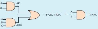
Prove the Boolean identity AC + ABC = AC and give its circuit description.
9.
In a transistor connected in the common base configuration, \(\alpha\) = 0 95, IE = 1 mA. Calculate the values of IC and IB.
10.
Explain the current flow in a NPN transistor.
11.
What do you mean by leakage current in a diode?
12.
State and prove De Morgan’s first and second theorem.
13.
Give circuit symbol, logical operation, truth table, and Boolean expression of
i) AND gate
ii) OR gate
iii) NOT gate
iv) NAND gate
v) NOR gate and
vi) EX-OR gate.
14.
What is electronics?
15.
Give the Schematic representation of valence band, conduction band, and forbidden energy gap and draw energy band structure of
(a) Insulators
(b) Semiconductors
(c) Metals?
16.
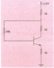
A transistor having α = 0.99 and VBE = 0.7V, is connected in the common-cmiitter configuration as shown in figure. If the transister is in saturation region, find the value of the collector current.
1.
(c)
Finite resistance which decreases with temperature
2.
(a)
Trivalent, neutral
3.
(c)
Signal phase reversal
4.
(c)
Photovoltaic action
5.
(d)
Voltage regulator
6.
A graph is plotted by taking the forward bias voltage (V) along the x- axis and the current (I) through the diode along y-axis. This graph is called the forward V-I characteristics.
7.
The internal repulsion of the depletion layer stops further diffusion of free electrons across the junction. This difference in potential across the depletion layer is called barrier potential.
8.
Step 1: AC (1 + B) = AC.1 [OR law-2]
Step 2: AC . 1 = AC [AND law – 2]
Therefore, AC + ABC = AC
Thus the Boolean identity is proved.
Circuit Description
9.
α = \(\frac{I_C}{I_E}\)
IC = α IE = 0.95 x 1 = 0.95 mA
IE = IB + IC
∴ IB = IE - IC = 1 - 0.95 = 0.05 mA
10.
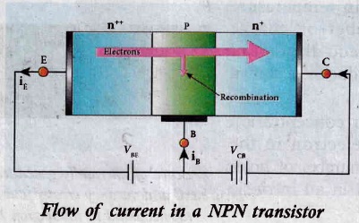
(i) The emitter-base junction is forward biased by a dc power supply Vm and the collector-based junction is reverse biased by the bias power supply VcB
(ii) The forward bias across the emitter base junction causes the majority charge carriers electrons in the emitter region to flow towards the base region and constitutes the emitter current (IE).
(iii) Since the base region is very narrow, most of the electrons reach the collector region.
(iv) The electrons that reach the collector region will be attracted by the collector terminal as it has positive potential and flows through the external circuit. This constitutes the collector current(Ic)
(v) The holes that are lost due to recombination in the base region ate replaced by the positive potential of the bias voltage VEE and constitute the base current (IB)
\( \mathrm{I}_{\mathrm{E}}=\mathrm{I}_{\mathrm{B}}+\mathrm{I}_{\mathrm{C}} \)
\(\mathrm{I}_{\mathrm{E}} \approx \mathrm{I}_{\mathrm{C}} \) \((\because \mathrm{I}_{\mathrm{B}} is\ very\ small )\)
11.
The leakage current is the current that the diode will leak when a reverse bias is applied to it.
12.
First Theorem :
The complement of the sum of two logical inputs is equal to the product of its complements.
\(\overline { A+B } \) = \(\bar { A } .\bar { B } \)
Proof:
(i) The Boolean equation for NOR gate is Y = \(\overline { A+B } \)
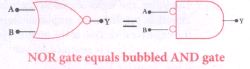
(ii) The Boolean equation for a bubbled AND gate is Y =\(\bar { A } .\bar { B } \)
(iii) Both cases generate same outputs for same inputs. It can be verified using the following truth
| A | B | A+B | \(\overline { A+B } \) | Ā | \(\bar { B } \) | \(\bar { A } .\bar { B } \) |
| 0 | 0 | 0 | 1 | 1 | 1 | 1 |
| 0 | 1 | 1 | 0 | 1 | 0 | 0 |
| 1 | 0 | 1 | 0 | 1 | 0 | 0 |
| 1 | 1 | 1 | 0 | 0 | 0 | 0 |
(i) From the above truth table, we can conclude \(\overline { A+B } \) = \(\bar { A } .\bar { B } \)
(ii) Thus De Morgan's first theorem is proved.
(iii) Hence, a NOR gate is equal to a bubbled AND gate
Second theorem :
The complement of the product of two is equal to the sum of its complements
\(\overline { A.B } \) = \(\bar { A } +\bar { B } \)
Proof:
(i) The Boolean equation for NAND gate is Y = \(\overline { A.B } \)
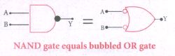
(ii) The Boolean equation for bubbled OR gate is Y = \(\bar { A } +\bar { B } \)
(iii) A and B are the inputs and Y is the output. The above two equations produces the same output for the same inputs. It can be verified by using the truth table.
| A | B | A+B | \(\overline{\mathrm{A}. \mathrm{B}}\) | Ā | \(\bar { B } \) | \(\overline{\mathrm{A}}+\overline{\mathrm{B}}\) |
| 0 | 0 | 0 | 1 | 1 | 1 | 1 |
| 0 | 1 | 0 | 1 | 1 | 0 | 1 |
| 1 | 0 | 0 | 1 | 0 | 1 | 1 |
| 1 | 1 | 1 | 0 | 0 | 0 | 0 |
(i) From the above truth table, we can conclude \(\overline { A.B } \) = \(\bar { A } +\bar { B } \)
(ii) Thus, De Morgan's second therom is proved.
(iii) Hence, a NAND gate is equal to a bubbled OR gate.
13.
i) AND gate
a) Circuit Symbol:
The circuit symbol of a two input AND gate is shown in Figure (a). A and B are inputs and Y is the output. It is a logic gate and hence A, B, and Y can have the value of either 1 or 0
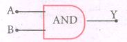
Two input AND gate
| Inputs | outputs | |
| A | B | Y = A + B |
| 0 | 0 | 0 |
| 0 | 1 | 0 |
| 1 | 0 | 0 |
| 1 | 1 | 1 |
Truth table
b) Boolean equation:
Y = A.B
It performs logical multiplication and is different from arithmetic multiplication.
c) Logic operation:
The output of AND gate is high only when all the inputs are high. In the rest of the cases, the output is low. It is represented in the truth table (Figure (b).
ii) OR gate
a) Circuit Symbol:
The circuit symbol of a two input OR gate is shown in Figure (a). A and B are inputs and Y is the output.
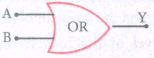
The input OR gate
| Inputs | outputs | |
| A | B | Y = A + B |
| 0 | 0 | 0 |
| 0 | 1 | 1 |
| 1 | 0 | 1 |
| 1 | 1 | 1 |
Truth table
a) Boolean equation:
A + B = Y
It performs logical addition and is different from arithmetic addition.
b) Logic operation:
The output of OR gate is high (logic 1 state) when either of the inputs or both are high. The truth table of OR gate is shown in Figure (a).
iii) NOT gate
a) Circuit Symbol:
The circuit symbol of NOT gate is shown in Figure (a). A and B are inputs and Y is the output.
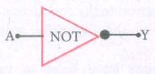
NOT gate
| Inputs | Output |
| A | Y = Ā |
| 0 | 1 |
| 1 | 0 |
Truth table
a) Boolean equation:
Y = Ā
b) Logic operation:
The output is the complement of the input. It is represented with an overbar. It is also called as inverter. The truth table infers that the output Y is I when input A is 0 and vice versa. The truth table of NOT is shown in Figure (b).
iv) NAND gate
a) Circuit Symbol:
The circuit symbol of NAND gate is shown in Figure (a). A and B are inputs and Y is the output.

Two input NAND gate
| Inputs | Output (AND) |
outputs (NAND) |
|
| A | B | Z = A.B | Y = \(\overline { A.B } \) |
| 0 | 0 | 0 | 1 |
| 0 | 1 | 0 | 1 |
| 1 | 0 | 0 | 1 |
| 1 | 1 | 1 | 0 |
Truth table
b) Boolean equation:
Y = \(\overline { A.B } \)
Logic operation:
The output Y equals, the complement of AND operation. The circuit is an AND gate followed by a NOT gate. Therefore, it is summarized as NAND. The output is at logic zero only when all the inputs are high. The rest of the cases, the output is high (Logic I state). The truth table of NAND gate is shown in Figure (b).
v) NOR gate
a) Circuit Symbol:
The circuit symbol of NOR gate is shown in Figure (a). A and B are inputs and Y is the output.

Two input NANS gate
| Inputs | Output (OR) |
outputs (NOR) |
|
| A | B | Z = A + B | Y = \(\overline { A+B } \) |
| 0 | 0 | 0 | 1 |
| 0 | 1 | 1 | 0 |
| 1 | 0 | 1 | 0 |
| 1 | 1 | 1 | 0 |
Truth table
Boolean equation:
Y = \(\overline { A+B } \)
Logic operation:
The output Y equals the complement of OR operation (A OR B). The circuit is an OR gate followed by a NOT gate and is summarized as NOR. The output is high when all the inputs are low. The output is low for all other combinations of inputs. The truth table of NOR gate is shown in Figure (b).
vi) Ex-OR gate
a) Circuit Symbol:
The circuit symbol of Ex-OR gate is shown in Figure (a). A and B are inputs and Y is the output. The Ex-OR operation is denoted as ⊕
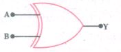
Ex-OR gate
| Inputs | outputs (Ex-OR) |
|
| A | B | Y = A ⊕ B |
| 0 | 0 | 0 |
| 0 | 1 | 1 |
| 1 | 0 | 1 |
| 1 | 1 | 0 |
Truth table
b) Boolean equation
Y = \(A.\overline { B } \) + \(\overline { A }.B \)
Y = A ⊕ B
Logic operation:
The output is high only when either of the two inputs is high. In the case of an Ex-OR gate with more than two inputs, the output will be high when odd number of inputs are high. The truth table of Ex-OR gate is shown in Figure (b).
14.
(i) It is the branch of physics incorporated with technology towards the design of circuits using transistors and microchips.
(ii) It depicts the behavior and movement of electrons in a semiconductor, vacuum, or gas.
(iii) Electronics deals with electrical circuits that involve active components such as transistors, diodes, integrated circuits, and sensors, associated with the passive components like resistors, inductors, capacitors, and transformers.
15.
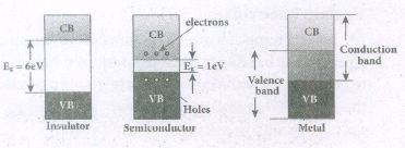
16.
\(\mathrm{V}_{\mathrm{cc}}=12 \mathrm{~V}, \mathrm{R}_{\mathrm{B}}=10 \mathrm{k} \Omega, \mathrm{R}_{\mathrm{E}}=1 \mathrm{k} \Omega, \mathrm{R}_{\mathrm{c}}=1+1=2 \mathrm{k} \Omega, \alpha=0.99, \mathrm{~V}_{\mathrm{BE}}=0.7 \mathrm{~V}, \mathrm{I}_{\mathrm{c}}=?\)
\(\beta=\alpha /(1-\alpha)=0.99 /(1-0.99)=99\)
\(\mathrm{I}_{\mathrm{B}}=\mathrm{I}_{\mathrm{C}} / \beta=\mathrm{I}_{\mathrm{c}} / 99\)
Applying Kirchoff's Voltage law,
\(I_C R_C+I_n R_n+I_E R_E+V_{u t}=V\)
\(2 \times 10^3 \mathrm{I}_{\mathrm{C}}+10 \times 10^3\left(\mathrm{I}_{\mathrm{C}} / 99\right)+1 \times 10^3\left(\mathrm{I}_{\mathrm{C}}+\mathrm{I}_{\mathrm{C}} / 99\right)+0.7=12 \quad\left(\because \mathrm{I}_{\mathrm{E}}=\mathrm{I}_{\mathrm{n}}+\mathrm{I}_{\mathrm{C}}\right)\)
\(\therefore \mathrm{I}_{\mathrm{C}}=\frac{11.3 \times 10^{-3} \times 99}{298}\)
\(\mathrm{I}_{\mathrm{C}}=3.7 \times 10^{-3} \mathrm{~A}=3.7 \mathrm{~mA}\)

12th Standard Syllabus & Materials
12th Standard
TN 12th Computer Applications களப்பெயர் முறைமை (DNS) Sample Question Papers Study Material - QB365 Set A
NEW12th Standard
TN 12th Computer Applications வலையமைப்பு எடுத்துக்காட்டுகள் மற்றும் நெறிமுறைகள் Sample Question Papers Study Material - QB365 Set A
NEW12th Standard
TN 12th Computer Applications கணினி வலையமைப்பு ஓர் அறிமுகம் Sample Question Papers Study Material - QB365 Set A
NEW12th Standard
TN 12th Computer Applications PHP-உடன் MySQL-ஐ இணைத்தல் Sample Question Papers Study Material - QB365 Set A



Tamilnadu Stateboard 12th Standard Subjects

Maths

Chemistry
Physics

Biology

Computer Science

Business Maths and Statistics

Economics

Commerce

Accountancy

History

Computer Applications
Biology
Computer Technology
Computer Applications
Computer Science
Business Maths and Statistics
Commerce
Economics
Maths
Chemistry
Physics
Computer Technology
History
Accountancy

Tamil

English

French
Tamilnadu Stateboard Standards

