
 100% FREE ACCESS
12th Standard Syllabus & Materials
12th Standard
TN 12th Computer Applications மின்னணு தரவு பரிமாற்றம் Sample Question Papers Study Material - QB365 Set A
NEW12th Standard
TN 12th Computer Applications மின் - வணிக பாதுகாப்பு அமைப்புகள் Sample Question Papers Study Material - QB365 Set A
NEW12th Standard
TN 12th Computer Applications மின்னணு செலுத்தல் முறைகள் Sample Question Papers Study Material - QB365 Set A
NEW12th Standard
TN 12th Computer Applications மின் - வணிகம் Sample Question Papers Study Material - QB365 Set A
NEW12th Standard
TN 12th Computer Applications திறந்த மூல கருத்துருக்கள் Sample Question Papers Study Material - QB365 Set A
NEW12th Standard
TN 12th Computer Applications வலையமைப்பு வடமிடல் Sample Question Papers Study Material - QB365 Set A

Published on: 02/11/2019
Semiconductor Electronics
Download Tamil Nadu 12th Standard Physics question papers, model tests, one-mark questions, important questions, and public exam papers in PDF format. Free study materials and answer keys for TN State Board students.
Questions + Answers key
Take MCQ Physics Test1.
2.
Explain the need for a feedback circuit in a transistor oscillator.
3.
What is the phase relationship between the AC input and output voltages in a common emitter amplifier? What is the reason for the phase reversal?
4.
Explain the current flow in a NPN transistor.
5.
Distinguish between avalanche breakdown and Zener breakdown.
6.
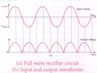
Draw the input and output waveform of a full wave rectifier.
7.
What do you mean by leakage current in a diode?
8.
A diode is called as a unidirectional device. Explain.
9.
What do you mean by doping?
10.
11.
Define electron motion in a semiconductor.
12.
Discuss the biasing polarities in an NPN and PNP transistors
13.
How electron-hole pairs are created in a semiconductor material?
14.
Give circuit symbol, logical operation, truth table, and Boolean expression of
i) AND gate
ii) OR gate
iii) NOT gate
iv) NAND gate
v) NOR gate and
vi) EX-OR gate.
1.
2.
(i) If the portion of the output fed to the input is in phase with the input, then the magnitude of the input signal increases
(ii) It is necessary for sustained oscillations.
3.
(i) The output signal is reversed by 180o. During the positive half cycle, Input signal (Vs) increases the forward voltage across the emitter-base.
(ii) As a resultthe base current (IB) increases. Consequently, the collector current (IC) increases ß times.
(iii) This increases the voltage drop across Rc (IC RC) which in turn decreases the collector-emitter voltage (VCE).
(iv) Therefore, the input signal in the positive direction produces an amplified signal in the negative direction at the output.
4.
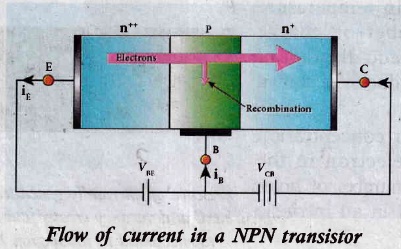
(i) The emitter-base junction is forward biased by a dc power supply Vm and the collector-based junction is reverse biased by the bias power supply VcB
(ii) The forward bias across the emitter base junction causes the majority charge carriers electrons in the emitter region to flow towards the base region and constitutes the emitter current (IE).
(iii) Since the base region is very narrow, most of the electrons reach the collector region.
(iv) The electrons that reach the collector region will be attracted by the collector terminal as it has positive potential and flows through the external circuit. This constitutes the collector current(Ic)
(v) The holes that are lost due to recombination in the base region ate replaced by the positive potential of the bias voltage VEE and constitute the base current (IB)
\( \mathrm{I}_{\mathrm{E}}=\mathrm{I}_{\mathrm{B}}+\mathrm{I}_{\mathrm{C}} \)
\(\mathrm{I}_{\mathrm{E}} \approx \mathrm{I}_{\mathrm{C}} \) \((\because \mathrm{I}_{\mathrm{B}} is\ very\ small )\)
5.
| S.No | Avalanche breakdown | Zener breakdown |
| (i) | Heavily doped p-n junctions have narrow depletion layers of the order of <10-6 m. | It occurs in lightly doped junctions Which have wide depletion layers. |
| (ii) | Electric field produced is strong in nature. | Weak electric field is produced. |
| (iii) | When a reverse voltage across the junction is increased to the breakdown limit, a very strong electric field is set up. It ruptures the covalent bonds in the lattice and thereby generating electronic-hole pairs. This effect is called Zener effect | Thermally generated minority charge carriers accelerated by the electric field gains sufficient kinetic energy, collide with the semiconductor atoms while passing through the depletion region. This leads to the breaking of covalent bonds and in turn covalent bonds and in turn generates electron-hole pairs |
| (iv) | Even a small further increases in reverse voltage produces a large number of charge carriers. Hence the junction has very low resistance in the breakdown region. | The newly generated charged carriers are also accelerated by the electric field resulting in more collisions and further production of charged carriers. |
| (v) | This process of emission of electrons due to the strong electric field is known as internal field emission or field ionization. | This cumulative process leads to an avalanche of charge carriers across the junction and consequently reduces the reverse resistance the diode current increases sharply. |
6.
7.
The leakage current is the current that the diode will leak when a reverse bias is applied to it.
8.
When a PN junction diode is forward biased, the depletion region decreases and the diode conduct once after the barrier potential is crossed, when it is reverse biased the depletion region increases and the diode does not conduct sci it is called as unidirectional device.
9.
The process of adding impurities to the instrinsic semiconductor is called doping.
10.
11.
(i) To move the hole in a given direction, the valence electrons move in the opposite direction.
(ii) Electrons flow in a N-type semiconductor is similar to electrons moving in a metallic wire.
(iii) The N- type dopant atoms will yield electrons available for conduction.
12.
(i) In NPN transistor, a positive voltage is given to the collector terminal to produce a current flow from the collector to the emitter.
(ii) In a PNP transistor, a positive voltage is given to the emitter terminal to produce current flow from the emitter to collector.
(iii) To operate the transistor in the active region, emitter-base must be forward biased and collector base must be reverse biased.
13.
(i) A Semiconductor in its pure form without impurity is called an intrinsic semiconductor.
(ii) Impurity means any other atom in the crystal lattice.
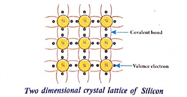
(iii) Each silicon atom has four electrons in the outmost orbit and is covalently bonded with the neighboring atoms to form the lattice. The band diagram is shown in the figure.
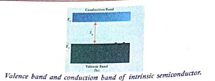
(iv) A small increase in temperature is sufficient enough to break some of the covalent bonds and release the electrons free from the lattices as shown in figure.
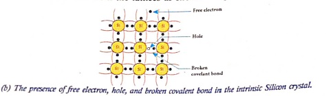
(v) The vacancies produced in the valence band are called holes. As the holes are dericiency of electrons, they are treated to possess positive charges Hence electrons and holes are the two charge carriers in semiconductors.
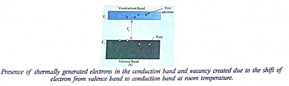
(vi) The number of electrons in the conduction band is equal to the number of holes in the valance band. The conduction is done to the electrons in the conduction band and holes in the valence band.
\(\begin{array}{l}
I=I_c+I_{\mathrm{h}} \\
I=\text { Total current } \\
I_e=\text { Electron current } \\
I_{\mathrm{h}}=\text { hole current }
\end{array}\)
(vii) It behaves like an insulator at 0 K. The increase in temperature increases the number of charge carriers.
(viii) The intrinsic carrier concentration is the number of electron in the conduction band or number of holes in the valence band in an intrinsic semi conductor.
14.
i) AND gate
a) Circuit Symbol:
The circuit symbol of a two input AND gate is shown in Figure (a). A and B are inputs and Y is the output. It is a logic gate and hence A, B, and Y can have the value of either 1 or 0
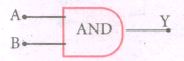
Two input AND gate
| Inputs | outputs | |
| A | B | Y = A + B |
| 0 | 0 | 0 |
| 0 | 1 | 0 |
| 1 | 0 | 0 |
| 1 | 1 | 1 |
Truth table
b) Boolean equation:
Y = A.B
It performs logical multiplication and is different from arithmetic multiplication.
c) Logic operation:
The output of AND gate is high only when all the inputs are high. In the rest of the cases, the output is low. It is represented in the truth table (Figure (b).
ii) OR gate
a) Circuit Symbol:
The circuit symbol of a two input OR gate is shown in Figure (a). A and B are inputs and Y is the output.
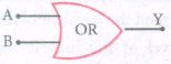
The input OR gate
| Inputs | outputs | |
| A | B | Y = A + B |
| 0 | 0 | 0 |
| 0 | 1 | 1 |
| 1 | 0 | 1 |
| 1 | 1 | 1 |
Truth table
a) Boolean equation:
A + B = Y
It performs logical addition and is different from arithmetic addition.
b) Logic operation:
The output of OR gate is high (logic 1 state) when either of the inputs or both are high. The truth table of OR gate is shown in Figure (a).
iii) NOT gate
a) Circuit Symbol:
The circuit symbol of NOT gate is shown in Figure (a). A and B are inputs and Y is the output.
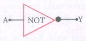
NOT gate
| Inputs | Output |
| A | Y = Ā |
| 0 | 1 |
| 1 | 0 |
Truth table
a) Boolean equation:
Y = Ā
b) Logic operation:
The output is the complement of the input. It is represented with an overbar. It is also called as inverter. The truth table infers that the output Y is I when input A is 0 and vice versa. The truth table of NOT is shown in Figure (b).
iv) NAND gate
a) Circuit Symbol:
The circuit symbol of NAND gate is shown in Figure (a). A and B are inputs and Y is the output.

Two input NAND gate
| Inputs | Output (AND) |
outputs (NAND) |
|
| A | B | Z = A.B | Y = \(\overline { A.B } \) |
| 0 | 0 | 0 | 1 |
| 0 | 1 | 0 | 1 |
| 1 | 0 | 0 | 1 |
| 1 | 1 | 1 | 0 |
Truth table
b) Boolean equation:
Y = \(\overline { A.B } \)
Logic operation:
The output Y equals, the complement of AND operation. The circuit is an AND gate followed by a NOT gate. Therefore, it is summarized as NAND. The output is at logic zero only when all the inputs are high. The rest of the cases, the output is high (Logic I state). The truth table of NAND gate is shown in Figure (b).
v) NOR gate
a) Circuit Symbol:
The circuit symbol of NOR gate is shown in Figure (a). A and B are inputs and Y is the output.

Two input NANS gate
| Inputs | Output (OR) |
outputs (NOR) |
|
| A | B | Z = A + B | Y = \(\overline { A+B } \) |
| 0 | 0 | 0 | 1 |
| 0 | 1 | 1 | 0 |
| 1 | 0 | 1 | 0 |
| 1 | 1 | 1 | 0 |
Truth table
Boolean equation:
Y = \(\overline { A+B } \)
Logic operation:
The output Y equals the complement of OR operation (A OR B). The circuit is an OR gate followed by a NOT gate and is summarized as NOR. The output is high when all the inputs are low. The output is low for all other combinations of inputs. The truth table of NOR gate is shown in Figure (b).
vi) Ex-OR gate
a) Circuit Symbol:
The circuit symbol of Ex-OR gate is shown in Figure (a). A and B are inputs and Y is the output. The Ex-OR operation is denoted as ⊕
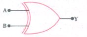
Ex-OR gate
| Inputs | outputs (Ex-OR) |
|
| A | B | Y = A ⊕ B |
| 0 | 0 | 0 |
| 0 | 1 | 1 |
| 1 | 0 | 1 |
| 1 | 1 | 0 |
Truth table
b) Boolean equation
Y = \(A.\overline { B } \) + \(\overline { A }.B \)
Y = A ⊕ B
Logic operation:
The output is high only when either of the two inputs is high. In the case of an Ex-OR gate with more than two inputs, the output will be high when odd number of inputs are high. The truth table of Ex-OR gate is shown in Figure (b).

12th Standard Syllabus & Materials
12th Standard
TN 12th Computer Applications களப்பெயர் முறைமை (DNS) Sample Question Papers Study Material - QB365 Set A
NEW12th Standard
TN 12th Computer Applications வலையமைப்பு எடுத்துக்காட்டுகள் மற்றும் நெறிமுறைகள் Sample Question Papers Study Material - QB365 Set A
NEW12th Standard
TN 12th Computer Applications கணினி வலையமைப்பு ஓர் அறிமுகம் Sample Question Papers Study Material - QB365 Set A
NEW12th Standard
TN 12th Computer Applications PHP-உடன் MySQL-ஐ இணைத்தல் Sample Question Papers Study Material - QB365 Set A



Tamilnadu Stateboard 12th Standard Subjects

Maths

Chemistry
Physics

Biology

Computer Science

Business Maths and Statistics

Economics

Commerce

Accountancy

History

Computer Applications
Biology
Computer Technology
Computer Applications
Computer Science
Business Maths and Statistics
Commerce
Economics
Maths
Chemistry
Physics
Computer Technology
History
Accountancy

Tamil

English

French
Tamilnadu Stateboard Standards

