
 100% FREE ACCESS
12th Standard Syllabus & Materials
12th Standard
TN 12th Computer Applications மின்னணு தரவு பரிமாற்றம் Sample Question Papers Study Material - QB365 Set A
NEW12th Standard
TN 12th Computer Applications மின் - வணிக பாதுகாப்பு அமைப்புகள் Sample Question Papers Study Material - QB365 Set A
NEW12th Standard
TN 12th Computer Applications மின்னணு செலுத்தல் முறைகள் Sample Question Papers Study Material - QB365 Set A
NEW12th Standard
TN 12th Computer Applications மின் - வணிகம் Sample Question Papers Study Material - QB365 Set A
NEW12th Standard
TN 12th Computer Applications திறந்த மூல கருத்துருக்கள் Sample Question Papers Study Material - QB365 Set A
NEW12th Standard
TN 12th Computer Applications வலையமைப்பு வடமிடல் Sample Question Papers Study Material - QB365 Set A

Published on: 22/01/2020
Semiconductor Electronics
Download Tamil Nadu 12th Standard Physics question papers, model tests, one-mark questions, important questions, and public exam papers in PDF format. Free study materials and answer keys for TN State Board students.
Questions + Answers key
Take MCQ Physics Test1.
Define depletion region.
2.
What is called logical variables?
3.
Define Zener effect
4.
What is rectification?
5.
Define forward bias.
6.
What is barrier potential?
7.
What is forbidden energy gap?
8.
9.
Explain the need for a feedback circuit in a transistor oscillator.
10.
What do you mean by leakage current in a diode?
11.
A diode is called as a unidirectional device. Explain.
12.
What do you mean by doping?
13.
14.
Discuss the biasing polarities in an NPN and PNP transistors
15.
Explain the working principle of a solar cell. Mention its applications.
1.
The electric field sweeps free carriers out of this region and hence it is called depletion region as it is depleted of free carriers.
2.
Digital electronics deals with logical operations. The variables are called logical variables
3.
Electric field is strong enough to break (or) rep tune the covalent bonds in the lattice and there by generating electron - hole pairs. This effect is called Zener effect.
4.
The process in which alternating voltage or alternating current is converted direct voltage or direct current is called rectification.
5.
If the positive terminal of the external voltage source is connected to the p-side and the negative terminal to the n-side, it is called forward bias.
6.
The internal repulsion of the depletion layer stops further diffusion of free electrons across the junction. This difference in potential across the depletion layer is called barrier potential.
7.
The energy gap between the valance band and conduction band is called forbidden energy gap
8.
9.
(i) If the portion of the output fed to the input is in phase with the input, then the magnitude of the input signal increases
(ii) It is necessary for sustained oscillations.
10.
The leakage current is the current that the diode will leak when a reverse bias is applied to it.
11.
When a PN junction diode is forward biased, the depletion region decreases and the diode conduct once after the barrier potential is crossed, when it is reverse biased the depletion region increases and the diode does not conduct sci it is called as unidirectional device.
12.
The process of adding impurities to the instrinsic semiconductor is called doping.
13.
14.
(i) In NPN transistor, a positive voltage is given to the collector terminal to produce a current flow from the collector to the emitter.
(ii) In a PNP transistor, a positive voltage is given to the emitter terminal to produce current flow from the emitter to collector.
(iii) To operate the transistor in the active region, emitter-base must be forward biased and collector base must be reverse biased.
15.
A solar cell, also known as photovoltaic cell, works on the principle of photovoltaic effect Accordingly, the p-n junction of the solar cell generates emf when solar radiation falls on it. The construction details and cross-sectional view are shown in Figure.
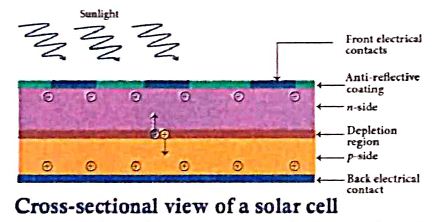
(i) In a solar cell, electron-hole pairs are generated due to the absorption of light near the junction.
(ii) Then the charge carriers are separated due to the electric field of the depletion region.
(iii) Electrons move towards n-type Silicon and holes move towards p-type Silicon layer.
(iv) The electrons reaching the n-side are collected by the front contact and holes reaching p-side are collected by the back electrical contact. Thus a potential difference is developed across solar cell.
(v) When an external load is connected to the solar cell, photocurrent flows through the load.
(vi) Many solar cells are connected together either in series or in parallel combination to form solar panel.
(vii) Many solar panels are connected with each other to form solar arrays.
(viii) For high power applications, solar panels and solar arrays are used.
Applications:
(i) Solar cells are widely used in calculators, watches, toys, portable power supplies, etc.
(ii) Solar cells are used in satellites and space applications.
(iii) Solar panels are used for commercial production of electricity.

12th Standard Syllabus & Materials
12th Standard
TN 12th Computer Applications களப்பெயர் முறைமை (DNS) Sample Question Papers Study Material - QB365 Set A
NEW12th Standard
TN 12th Computer Applications வலையமைப்பு எடுத்துக்காட்டுகள் மற்றும் நெறிமுறைகள் Sample Question Papers Study Material - QB365 Set A
NEW12th Standard
TN 12th Computer Applications கணினி வலையமைப்பு ஓர் அறிமுகம் Sample Question Papers Study Material - QB365 Set A
NEW12th Standard
TN 12th Computer Applications PHP-உடன் MySQL-ஐ இணைத்தல் Sample Question Papers Study Material - QB365 Set A



Tamilnadu Stateboard 12th Standard Subjects

Maths

Chemistry
Physics

Biology

Computer Science

Business Maths and Statistics

Economics

Commerce

Accountancy

History

Computer Applications
Biology
Computer Technology
Computer Applications
Computer Science
Business Maths and Statistics
Commerce
Economics
Maths
Chemistry
Physics
Computer Technology
History
Accountancy

Tamil

English

French
Tamilnadu Stateboard Standards

