
 100% FREE ACCESS
12th Standard Syllabus & Materials
12th Standard
TN 12th Computer Applications மின்னணு தரவு பரிமாற்றம் Sample Question Papers Study Material - QB365 Set A
NEW12th Standard
TN 12th Computer Applications மின் - வணிக பாதுகாப்பு அமைப்புகள் Sample Question Papers Study Material - QB365 Set A
NEW12th Standard
TN 12th Computer Applications மின்னணு செலுத்தல் முறைகள் Sample Question Papers Study Material - QB365 Set A
NEW12th Standard
TN 12th Computer Applications மின் - வணிகம் Sample Question Papers Study Material - QB365 Set A
NEW12th Standard
TN 12th Computer Applications திறந்த மூல கருத்துருக்கள் Sample Question Papers Study Material - QB365 Set A
NEW12th Standard
TN 12th Computer Applications வலையமைப்பு வடமிடல் Sample Question Papers Study Material - QB365 Set A

Published on: 13/05/2022
QB365 provides detailed and simple solution for every Book back Questions in class 12 Physics Subject. It will helps to get more idea about question pattern in every book back questions with solution.
latest Book back QuestionsDownload Tamil Nadu 12th Standard Physics question papers, model tests, one-mark questions, important questions, and public exam papers in PDF format. Free study materials and answer keys for TN State Board students.
Questions + Answers key
Take MCQ Physics Test1.
Discuss the biasing polarities in an NPN and PNP transistors
2.
What is mobile communication?
3.
Define bandwidth of transmission system.
4.
What is the phase relationship between the AC input and output voltages in a common emitter amplifier? What is the reason for the phase reversal?
5.
Give circuit symbol, logical operation, truth table, and Boolean expression of
i) AND gate
ii) OR gate
iii) NOT gate
iv) NAND gate
v) NOR gate and
vi) EX-OR gate.
1.
(i) In NPN transistor, a positive voltage is given to the collector terminal to produce a current flow from the collector to the emitter.
(ii) In a PNP transistor, a positive voltage is given to the emitter terminal to produce current flow from the emitter to collector.
(iii) To operate the transistor in the active region, emitter-base must be forward biased and collector base must be reverse biased.
2.
Mobile communication is used to communicate with others in different locations without the use of any physical connection like wires or cables.
3.
The range of frequencies required to transmit a piece of specified information in a particular channel is called channel bandwidth or the bandwidth of the transmission system.
4.
(i) The output signal is reversed by 180o. During the positive half cycle, Input signal (Vs) increases the forward voltage across the emitter-base.
(ii) As a resultthe base current (IB) increases. Consequently, the collector current (IC) increases ß times.
(iii) This increases the voltage drop across Rc (IC RC) which in turn decreases the collector-emitter voltage (VCE).
(iv) Therefore, the input signal in the positive direction produces an amplified signal in the negative direction at the output.
5.
i) AND gate
a) Circuit Symbol:
The circuit symbol of a two input AND gate is shown in Figure (a). A and B are inputs and Y is the output. It is a logic gate and hence A, B, and Y can have the value of either 1 or 0
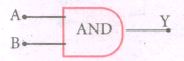
Two input AND gate
| Inputs | outputs | |
| A | B | Y = A + B |
| 0 | 0 | 0 |
| 0 | 1 | 0 |
| 1 | 0 | 0 |
| 1 | 1 | 1 |
Truth table
b) Boolean equation:
Y = A.B
It performs logical multiplication and is different from arithmetic multiplication.
c) Logic operation:
The output of AND gate is high only when all the inputs are high. In the rest of the cases, the output is low. It is represented in the truth table (Figure (b).
ii) OR gate
a) Circuit Symbol:
The circuit symbol of a two input OR gate is shown in Figure (a). A and B are inputs and Y is the output.
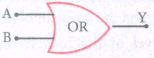
The input OR gate
| Inputs | outputs | |
| A | B | Y = A + B |
| 0 | 0 | 0 |
| 0 | 1 | 1 |
| 1 | 0 | 1 |
| 1 | 1 | 1 |
Truth table
a) Boolean equation:
A + B = Y
It performs logical addition and is different from arithmetic addition.
b) Logic operation:
The output of OR gate is high (logic 1 state) when either of the inputs or both are high. The truth table of OR gate is shown in Figure (a).
iii) NOT gate
a) Circuit Symbol:
The circuit symbol of NOT gate is shown in Figure (a). A and B are inputs and Y is the output.
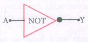
NOT gate
| Inputs | Output |
| A | Y = Ā |
| 0 | 1 |
| 1 | 0 |
Truth table
a) Boolean equation:
Y = Ā
b) Logic operation:
The output is the complement of the input. It is represented with an overbar. It is also called as inverter. The truth table infers that the output Y is I when input A is 0 and vice versa. The truth table of NOT is shown in Figure (b).
iv) NAND gate
a) Circuit Symbol:
The circuit symbol of NAND gate is shown in Figure (a). A and B are inputs and Y is the output.

Two input NAND gate
| Inputs | Output (AND) |
outputs (NAND) |
|
| A | B | Z = A.B | Y = \(\overline { A.B } \) |
| 0 | 0 | 0 | 1 |
| 0 | 1 | 0 | 1 |
| 1 | 0 | 0 | 1 |
| 1 | 1 | 1 | 0 |
Truth table
b) Boolean equation:
Y = \(\overline { A.B } \)
Logic operation:
The output Y equals, the complement of AND operation. The circuit is an AND gate followed by a NOT gate. Therefore, it is summarized as NAND. The output is at logic zero only when all the inputs are high. The rest of the cases, the output is high (Logic I state). The truth table of NAND gate is shown in Figure (b).
v) NOR gate
a) Circuit Symbol:
The circuit symbol of NOR gate is shown in Figure (a). A and B are inputs and Y is the output.

Two input NANS gate
| Inputs | Output (OR) |
outputs (NOR) |
|
| A | B | Z = A + B | Y = \(\overline { A+B } \) |
| 0 | 0 | 0 | 1 |
| 0 | 1 | 1 | 0 |
| 1 | 0 | 1 | 0 |
| 1 | 1 | 1 | 0 |
Truth table
Boolean equation:
Y = \(\overline { A+B } \)
Logic operation:
The output Y equals the complement of OR operation (A OR B). The circuit is an OR gate followed by a NOT gate and is summarized as NOR. The output is high when all the inputs are low. The output is low for all other combinations of inputs. The truth table of NOR gate is shown in Figure (b).
vi) Ex-OR gate
a) Circuit Symbol:
The circuit symbol of Ex-OR gate is shown in Figure (a). A and B are inputs and Y is the output. The Ex-OR operation is denoted as ⊕
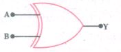
Ex-OR gate
| Inputs | outputs (Ex-OR) |
|
| A | B | Y = A ⊕ B |
| 0 | 0 | 0 |
| 0 | 1 | 1 |
| 1 | 0 | 1 |
| 1 | 1 | 0 |
Truth table
b) Boolean equation
Y = \(A.\overline { B } \) + \(\overline { A }.B \)
Y = A ⊕ B
Logic operation:
The output is high only when either of the two inputs is high. In the case of an Ex-OR gate with more than two inputs, the output will be high when odd number of inputs are high. The truth table of Ex-OR gate is shown in Figure (b).

12th Standard Syllabus & Materials
12th Standard
TN 12th Computer Applications களப்பெயர் முறைமை (DNS) Sample Question Papers Study Material - QB365 Set A
NEW12th Standard
TN 12th Computer Applications வலையமைப்பு எடுத்துக்காட்டுகள் மற்றும் நெறிமுறைகள் Sample Question Papers Study Material - QB365 Set A
NEW12th Standard
TN 12th Computer Applications கணினி வலையமைப்பு ஓர் அறிமுகம் Sample Question Papers Study Material - QB365 Set A
NEW12th Standard
TN 12th Computer Applications PHP-உடன் MySQL-ஐ இணைத்தல் Sample Question Papers Study Material - QB365 Set A



Tamilnadu Stateboard 12th Standard Subjects

Maths

Chemistry
Physics

Biology

Computer Science

Business Maths and Statistics

Economics

Commerce

Accountancy

History

Computer Applications
Biology
Computer Technology
Computer Applications
Computer Science
Business Maths and Statistics
Commerce
Economics
Maths
Chemistry
Physics
Computer Technology
History
Accountancy

Tamil

English

French
Tamilnadu Stateboard Standards



