
 100% FREE ACCESS
12th Standard Syllabus & Materials
12th Standard
TN 12th Maths Applications of Matrices and Determinants Sample Question Papers Study Material - QB365 Set A
NEW12th Standard
TN 12th Computer Applications மின்னணு தரவு பரிமாற்றம் Sample Question Papers Study Material - QB365 Set A
NEW12th Standard
TN 12th Computer Applications மின் - வணிக பாதுகாப்பு அமைப்புகள் Sample Question Papers Study Material - QB365 Set A
NEW12th Standard
TN 12th Computer Applications மின்னணு செலுத்தல் முறைகள் Sample Question Papers Study Material - QB365 Set A
NEW12th Standard
TN 12th Computer Applications மின் - வணிகம் Sample Question Papers Study Material - QB365 Set A
NEW12th Standard
TN 12th Computer Applications திறந்த மூல கருத்துருக்கள் Sample Question Papers Study Material - QB365 Set A

Published on: 01/06/2021
QB365 provides detailed and simple solution for every Book back Questions in class 12 Physics Subject. It will helps to get more idea about question pattern in every book back questions with solution.
Download Tamil Nadu 12th Standard Physics question papers, model tests, one-mark questions, important questions, and public exam papers in PDF format. Free study materials and answer keys for TN State Board students.
Questions + Answers key
Take MCQ Physics Test1.
How electron-hole pairs are created in a semiconductor material?
2.
What do you mean by Internet of Things?
3.
Distinguish between avalanche breakdown and Zener breakdown.
4.
What do you mean by leakage current in a diode?
5.
1.
(i) A Semiconductor in its pure form without impurity is called an intrinsic semiconductor.
(ii) Impurity means any other atom in the crystal lattice.
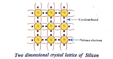
(iii) Each silicon atom has four electrons in the outmost orbit and is covalently bonded with the neighboring atoms to form the lattice. The band diagram is shown in the figure.
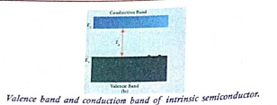
(iv) A small increase in temperature is sufficient enough to break some of the covalent bonds and release the electrons free from the lattices as shown in figure.
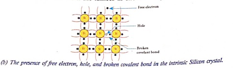
(v) The vacancies produced in the valence band are called holes. As the holes are dericiency of electrons, they are treated to possess positive charges Hence electrons and holes are the two charge carriers in semiconductors.
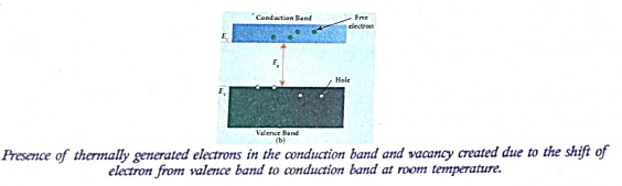
(vi) The number of electrons in the conduction band is equal to the number of holes in the valance band. The conduction is done to the electrons in the conduction band and holes in the valence band.
\(\begin{array}{l}
I=I_c+I_{\mathrm{h}} \\
I=\text { Total current } \\
I_e=\text { Electron current } \\
I_{\mathrm{h}}=\text { hole current }
\end{array}\)
(vii) It behaves like an insulator at 0 K. The increase in temperature increases the number of charge carriers.
(viii) The intrinsic carrier concentration is the number of electron in the conduction band or number of holes in the valence band in an intrinsic semi conductor.
2.
i) Internet is a fast-growing technology in the field of a communication system with multifaceted tools.
ii) It provides new ways and means to interact and connect with people.
iii) Internet is the largest computer network recognized globally that connects millions of people through computers.
iv) It finds extensive applications in all walks of life.
3.
| S.No | Avalanche breakdown | Zener breakdown |
| (i) | Heavily doped p-n junctions have narrow depletion layers of the order of <10-6 m. | It occurs in lightly doped junctions Which have wide depletion layers. |
| (ii) | Electric field produced is strong in nature. | Weak electric field is produced. |
| (iii) | When a reverse voltage across the junction is increased to the breakdown limit, a very strong electric field is set up. It ruptures the covalent bonds in the lattice and thereby generating electronic-hole pairs. This effect is called Zener effect | Thermally generated minority charge carriers accelerated by the electric field gains sufficient kinetic energy, collide with the semiconductor atoms while passing through the depletion region. This leads to the breaking of covalent bonds and in turn covalent bonds and in turn generates electron-hole pairs |
| (iv) | Even a small further increases in reverse voltage produces a large number of charge carriers. Hence the junction has very low resistance in the breakdown region. | The newly generated charged carriers are also accelerated by the electric field resulting in more collisions and further production of charged carriers. |
| (v) | This process of emission of electrons due to the strong electric field is known as internal field emission or field ionization. | This cumulative process leads to an avalanche of charge carriers across the junction and consequently reduces the reverse resistance the diode current increases sharply. |
4.
The leakage current is the current that the diode will leak when a reverse bias is applied to it.
5.

12th Standard Syllabus & Materials
12th Standard
TN 12th Computer Applications வலையமைப்பு வடமிடல் Sample Question Papers Study Material - QB365 Set A
NEW12th Standard
TN 12th Computer Applications களப்பெயர் முறைமை (DNS) Sample Question Papers Study Material - QB365 Set A
NEW12th Standard
TN 12th Computer Applications வலையமைப்பு எடுத்துக்காட்டுகள் மற்றும் நெறிமுறைகள் Sample Question Papers Study Material - QB365 Set A
NEW12th Standard
TN 12th Computer Applications கணினி வலையமைப்பு ஓர் அறிமுகம் Sample Question Papers Study Material - QB365 Set A



Tamilnadu Stateboard 12th Standard Subjects

Maths

Chemistry
Physics

Biology

Computer Science

Business Maths and Statistics

Economics

Commerce

Accountancy

History

Computer Applications
Biology
Computer Technology
Computer Applications
Computer Science
Business Maths and Statistics
Commerce
Economics
Maths
Chemistry
Physics
Computer Technology
History
Accountancy

Tamil

English

French
Tamilnadu Stateboard Standards



