
 100% FREE ACCESS
12th Standard Syllabus & Materials
12th Standard
TN 12th Maths Applications of Matrices and Determinants Sample Question Papers Study Material - QB365 Set A
NEW12th Standard
TN 12th Computer Applications மின்னணு தரவு பரிமாற்றம் Sample Question Papers Study Material - QB365 Set A
NEW12th Standard
TN 12th Computer Applications மின் - வணிக பாதுகாப்பு அமைப்புகள் Sample Question Papers Study Material - QB365 Set A
NEW12th Standard
TN 12th Computer Applications மின்னணு செலுத்தல் முறைகள் Sample Question Papers Study Material - QB365 Set A
NEW12th Standard
TN 12th Computer Applications மின் - வணிகம் Sample Question Papers Study Material - QB365 Set A
NEW12th Standard
TN 12th Computer Applications திறந்த மூல கருத்துருக்கள் Sample Question Papers Study Material - QB365 Set A

Published on: 02/09/2022
QB365 provides a detailed and simple solution for every Possible Book Back Questions in Class 12 Physics Subject - Retirement and Death of a Partner, English Medium. It will help Students to get more practice questions, Students can Practice these question papers in addition to score best marks.
Download Tamil Nadu 12th Standard Physics question papers, model tests, one-mark questions, important questions, and public exam papers in PDF format. Free study materials and answer keys for TN State Board students.
Questions + Answers key
Take MCQ Physics Test1.
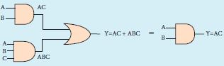
Prove the Boolean identity AC + ABC = AC and give its circuit description.
2.
In the combination of the following gates, write the Boolean equation for output Y in terms of inputs A and B.
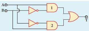
3.
What is the output Y in the following circuit, when all the three inputs A, B, and C are first 0 and then 1?
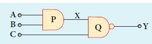
4.
In the circuit shown in the figure, the input voltage Vi is 20 V, VBE = 0 V, and VCE = 0 V. What are the values of IB, IC, β?
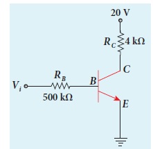
5.
In a transistor connected in the common base configuration, \(\alpha\) = 0 95, IE = 1 mA. Calculate the values of IC and IB.
6.
Determine the wavelength of light emitted from LED which is made up of GaAsP semiconductor whose forbidden energy gap is 1.875 eV. Mention the colour of the light emitted (Take h = 6.6 x 10⁻³⁴ Js).
7.
A silicon diode is connected with 1kΩ resistor as shown. Find the value of current flowing through AB is
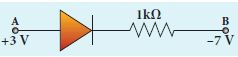
8.
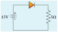
An ideal diode and a 5 Ω resistor are connected in series with a 15 V power supply as shown in figure below. Calculate the current that flows through the diode.
9.
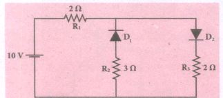
The given circuit has two ideal diodes connected as shown in figure below. Calculate the current flowing through the resistance R1.
10.
11.
Explain the need for a feedback circuit in a transistor oscillator.
12.
What is the phase relationship between the AC input and output voltages in a common emitter amplifier? What is the reason for the phase reversal?
13.
Explain the current flow in a NPN transistor.
14.
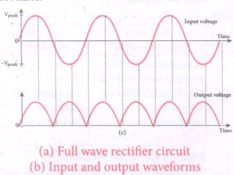
Draw the input and output waveform of a full wave rectifier.
15.
What do you mean by leakage current in a diode?
16.
A diode is called as a unidirectional device. Explain.
17.
What do you mean by doping?
18.
Define electron motion in a semiconductor.
19.
What does RADAR stand for?
20.
Explain centre frequency or resting frequency in frequency modulation.
21.
Give the factors that are responsible for transmission impairments.
22.
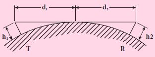
A transmitting antenna has a height of 40 m and the height of the receiving antenna is 30 m. What is the maximum distance between them for line-of-sight communication? The radius of the earth is 6.4 × 10⁶ m.
1.
Step 1: AC (1 + B) = AC.1 [OR law-2]
Step 2: AC . 1 = AC [AND law – 2]
Therefore, AC + ABC = AC
Thus the Boolean identity is proved.
Circuit Description
2.
The output at the 1st AND gate : A\(\overline { B } \)
The output at the 2nd AND gate : ĀB
The output at the OR gate: Y = A. \(\overline { B } \) + Ā .B
3.
| A | B | C | X = A.B | Y=\(\overline { X.C } \) |
| 0 | 0 | 0 | 0 | 1 |
| 1 | 1 | 1 | 1 | 0 |
4.
\({ I }_{ B }=\frac { { V }_{ i } }{ { R }_{ B } } =\frac { 20V }{ 500k\Omega } =40\mu A\) [∵ VBE = 0V]
\({ I }_{ C }=\frac { { V }_{ CC } }{ { R }_{ C } } =\frac { 20V }{ 4k\Omega } =5mA\) [∵ VCE = 0V]
\(\beta =\frac { { I }_{ C } }{ { I }_{ B } } =\frac { 5mA }{ 40\mu A } =125\)
5.
α = \(\frac{I_C}{I_E}\)
IC = α IE = 0.95 x 1 = 0.95 mA
IE = IB + IC
∴ IB = IE - IC = 1 - 0.95 = 0.05 mA
6.
\({ E }_{ g }=\frac { hc }{ \lambda } \)
Therefore,
\(\lambda =\frac { hc }{ { E }_{ g } } =\frac { 6.6\times { 10 }^{ -34 }\times 3\times { 10 }^{ 8 } }{ 1.875\times 1.6\times { 10 }^{ -19 } } \)
= 660 nm
The wavelength 660 nm corresponds to red colour light
7.
The P.D. between A and B is given by
\(V =\left[V_{\mathrm{A}}-V_{\mathrm{B}}\right]-V_{\mathrm{b}}(\mathrm{Si}) \)
\(=[3.3-(-7.4)]-0.7 \)
\(=10.7-0.7=10 \mathrm{~V} \)
The value of current flowing through AB can be obtained by using Ohm’s law
\(I=\frac { V }{ R } =\frac { 10}{ 1\times { 10 }^{ 3 } } ={ 10 }^{ -2 }A=10mA\)
8.
The diode is forward biased and it is an ideal one. Hence, it acts like a closed switch with no barrier voltage. Therefore, current that flows through the diode can be calculated using Ohm’s law.
V = IR
\(I=\frac{V}{R}=\frac{15}{5}\) = 3A
9.
V= 10V, R1 = 2 Ω, R3 = 2 Ω
Diode D1 is reverse biased so it will block the current and diode D2 is forward biased, so it will pass the current.
\(\mathrm{R} =\mathrm{R}_{1}+\mathrm{R}_{2} \)
\(=2+2=4 \Omega \)
\(\mathrm{I} =\frac{\mathrm{V}}{\mathrm{R}}=\frac{10}{4} \)
I = 2.5 A
10.
11.
(i) If the portion of the output fed to the input is in phase with the input, then the magnitude of the input signal increases
(ii) It is necessary for sustained oscillations.
12.
(i) The output signal is reversed by 180o. During the positive half cycle, Input signal (Vs) increases the forward voltage across the emitter-base.
(ii) As a resultthe base current (IB) increases. Consequently, the collector current (IC) increases ß times.
(iii) This increases the voltage drop across Rc (IC RC) which in turn decreases the collector-emitter voltage (VCE).
(iv) Therefore, the input signal in the positive direction produces an amplified signal in the negative direction at the output.
13.
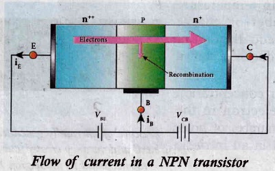
(i) The emitter-base junction is forward biased by a dc power supply Vm and the collector-based junction is reverse biased by the bias power supply VcB
(ii) The forward bias across the emitter base junction causes the majority charge carriers electrons in the emitter region to flow towards the base region and constitutes the emitter current (IE).
(iii) Since the base region is very narrow, most of the electrons reach the collector region.
(iv) The electrons that reach the collector region will be attracted by the collector terminal as it has positive potential and flows through the external circuit. This constitutes the collector current(Ic)
(v) The holes that are lost due to recombination in the base region ate replaced by the positive potential of the bias voltage VEE and constitute the base current (IB)
\( \mathrm{I}_{\mathrm{E}}=\mathrm{I}_{\mathrm{B}}+\mathrm{I}_{\mathrm{C}} \)
\(\mathrm{I}_{\mathrm{E}} \approx \mathrm{I}_{\mathrm{C}} \) \((\because \mathrm{I}_{\mathrm{B}} is\ very\ small )\)
14.
15.
The leakage current is the current that the diode will leak when a reverse bias is applied to it.
16.
When a PN junction diode is forward biased, the depletion region decreases and the diode conduct once after the barrier potential is crossed, when it is reverse biased the depletion region increases and the diode does not conduct sci it is called as unidirectional device.
17.
The process of adding impurities to the instrinsic semiconductor is called doping.
18.
(i) To move the hole in a given direction, the valence electrons move in the opposite direction.
(ii) Electrons flow in a N-type semiconductor is similar to electrons moving in a metallic wire.
(iii) The N- type dopant atoms will yield electrons available for conduction.
19.
RADAR stands for RAdio Detection And Ranging.
20.
When the frequency of the baseband signal is zero (no input signal), there is no change in the frequency of the carrier wave. It is at its normal frequency. This is called centre frequency or resting frequency.
21.
i) Noise : Interference of undesirable electrical signal with the transmitted signal.
ii) Attenuation: Loss of strength of a signal.
iii) Medium : It makes some distortion tothe signal.
22.
The total distance d between the transmitting and receiving antennas will be the sum of the individual distances of coverage.
d = d1 + d2
\(=\sqrt { 2R{ h }_{ 1 } } +\sqrt { 2{ Rh }_{ 2 } } \)
\(=\sqrt { 2R } \left( \sqrt { { h }_{ 1 } } +\sqrt { { h }_{ 2 } } \right) \)
\(=\sqrt { 2\times 6.4\times { 10 }^{ 6 } } \times (\sqrt { 40 } +\sqrt { 30 } )\)
\(=16\times { 10 }^{ 2 }\sqrt { 5 } \times (6.32+5.48)\)
= 42217 m = 42.217 km

12th Standard Syllabus & Materials
12th Standard
TN 12th Computer Applications வலையமைப்பு வடமிடல் Sample Question Papers Study Material - QB365 Set A
NEW12th Standard
TN 12th Computer Applications களப்பெயர் முறைமை (DNS) Sample Question Papers Study Material - QB365 Set A
NEW12th Standard
TN 12th Computer Applications வலையமைப்பு எடுத்துக்காட்டுகள் மற்றும் நெறிமுறைகள் Sample Question Papers Study Material - QB365 Set A
NEW12th Standard
TN 12th Computer Applications கணினி வலையமைப்பு ஓர் அறிமுகம் Sample Question Papers Study Material - QB365 Set A



Tamilnadu Stateboard 12th Standard Subjects

Maths

Chemistry
Physics

Biology

Computer Science

Business Maths and Statistics

Economics

Commerce

Accountancy

History

Computer Applications
Biology
Computer Technology
Computer Applications
Computer Science
Business Maths and Statistics
Commerce
Economics
Maths
Chemistry
Physics
Computer Technology
History
Accountancy

Tamil

English

French
Tamilnadu Stateboard Standards

