
 100% FREE ACCESS
12th Standard Syllabus & Materials
12th Standard
TN 12th Computer Applications மின்னணு தரவு பரிமாற்றம் Sample Question Papers Study Material - QB365 Set A
NEW12th Standard
TN 12th Computer Applications மின் - வணிக பாதுகாப்பு அமைப்புகள் Sample Question Papers Study Material - QB365 Set A
NEW12th Standard
TN 12th Computer Applications மின்னணு செலுத்தல் முறைகள் Sample Question Papers Study Material - QB365 Set A
NEW12th Standard
TN 12th Computer Applications மின் - வணிகம் Sample Question Papers Study Material - QB365 Set A
NEW12th Standard
TN 12th Computer Applications திறந்த மூல கருத்துருக்கள் Sample Question Papers Study Material - QB365 Set A
NEW12th Standard
TN 12th Computer Applications வலையமைப்பு வடமிடல் Sample Question Papers Study Material - QB365 Set A

Published on: 02/09/2022
QB365 provides a detailed and simple solution for every Possible Creative Questions in Class 12 Physics Subject - Retirement and Death of a Partner, English Medium. It will help Students to get more practice questions, Students can Practice these question papers in addition to score best marks.
Download Tamil Nadu 12th Standard Physics question papers, model tests, one-mark questions, important questions, and public exam papers in PDF format. Free study materials and answer keys for TN State Board students.
Questions + Answers key
Take MCQ Physics Test1.
In the following diagrams, indicate which of the diodes are forward biased and which reverse biased?

2.
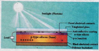
What is a solar cell? Draw the cross-sectional view of a solar cell and explain its consumption and working. Write a note on solar arrays.
3.
Calculate the voltage of resistors RB in the circuit shown to put VCE at 3.0 V.
4.
Draw the block diagram of transistor oscillators and explain it. (or) Explain the working of the transistor as on oscillator.
5.
What is meant by satellite communication? Give its applications.
6.
Write the applications of mobile communication.
7.
What is RADAR? Explain its function. State its applications
8.
For a BJT circuit shown, assume that the 'β' of the transistor is very large and VBE= 0.7 V. The mode of operation.
9.
For a BJT, the common - base current gain α = 0.98 and the collector base junction reverse bias saturation ICU = 0.6μA. This BJT is connected in the common emitter mode and operated in the active region with a base drive current ID= 20 μA. The collector current IC for this mode of operating is
10.
Write any two distinguishing features between Insulators, Metals and semiconductors and insulators an the basis of energy band diagrams.
11.
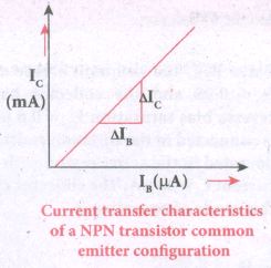
Explain current transfer characteristics.
12.
Explain and classify transistor as an oscillator.
13.
How does the change in temperature and application of electric field affect the behavior of materials and write the range of resistivity for each materials.
1.
This diode symbol is .jpg)
(i) For forward biased positive terminal of the battery connected to positive terminal of diode (or) negative terminal of battery connected to negative terminal of diode.
(ii) For reverse biased the polarities of battery and the diode are reversed. According to this, for our given diagram (a) is forward biased, (b) and (c) are reverse biased.
2.
A solar cell, also known as photovoltaic cell, converts light energy directly into electricity or electric potential difference by photovoltaic effect. It is basically a p-n junction which generates emf when solar radiation falls on the p-n junction. A solar cell is of two types: p-type and n-type.
Both types use a combination of p-type and n-type Silicon which together forms the p-n junction of the solar cell. The difference is that p type solar cells use p-type Silicon as the base with an ultra-thin layer of n-type Silicon as shown in Figure. While n-type solar cell uses the opposite combination. The other side of the p-silicon is coated with metal which forms the back electrical contact. On top of the n-type Silicon, metal grid is deposited which acts as the front electrical contact. The top of the solar cell is coated with anti-reflection coating and toughened glass.
In a solar cell, electron-hole pairs are generated due to the absorption of light near. the junction. Then the charge carriers are separated due to the electric field of the depletion region. Electrons moye towards n-type Silicon and holes move towards p-type Silicon layer. The electrons reaching the n-side are collected by the front contact and holes reaching p-side are collected by the back electrical contact. Thus a potential difference is developed across solar cell. When an external load is connected to the solar cell, photocurrent flows through the load.
Many solar cells are connected together either in series or in parallel combination to form solar panel or module. Many solar panels are connected with each other to form solar arrays. For high power applications, solar panels and solar arrays are used.
Applications:
(i) Solar cells are widely used in calculators, watches toys, portable power supplies, etc.
(ii) Solar cells are used in satellites and space applications.
(iii) Solar panels are used to generate electricity.
3.
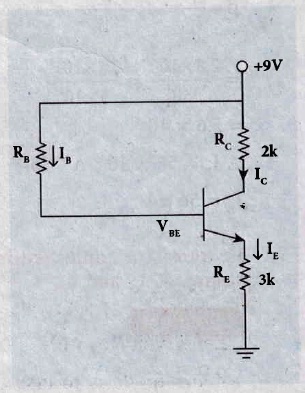
(VBE = 0.7 v and \(\beta\) = 80)
Apply KVL in Base - emitter loop
\(
\mathrm{R}_{\mathrm{B}} \mathrm{I}_{\mathrm{B}}+\mathrm{V}_{\mathrm{BE}}+\mathrm{R}_{\mathrm{E}} \mathrm{I}_{\mathrm{E}}=\mathrm{V}_{\mathrm{CC}}
\)
\(\mathrm{V}_{\mathrm{BE}}=0.7 \mathrm{~V}, \mathrm{I}_{\mathrm{C}}=\mathrm{I}_{\mathrm{E}}
\)
\(\mathrm{I}_{\mathrm{B}}=\frac{\mathrm{I}_{\mathrm{c}}}{\beta}=\frac{\mathrm{I}_{\mathrm{c}}}{80}\)
Substituting these in above equation, and taking resistance in k\(\Omega\)
\(R_{B} \frac{I_{c}}{80}+3 k \times I_{C}=V_{C C}-V_{B E}\)
= 94.7 = 8.3
\(R_{B} \frac{I_{c}}{80}+3 k \times I_{C}=8.3\) ....(1)
Applying in CE loop
\(\mathrm{I}_{\mathrm{C}} \mathrm{R}_{\mathrm{C}}+\mathrm{V}_{\mathrm{CE}}+\mathrm{I}_{\mathrm{E}} \times 3 \mathrm{k}=9 \mathrm{~V}\)
\(
I_{c} \times 2 k+3.0+I_{c} \times 3 \mathrm{k}=9 \mathrm{~V}
\)
\(I_{c}=\frac{6}{5 k}=1.2 \mathrm{~mA}\) .........(2)
Substitute (2) in (1)
\(
\mathrm{R}_{\mathrm{B}} \frac{1.2}{80}+3 \mathrm{k} \times 1.2 \mathrm{~mA}=8.3 \mathrm{~V}
\)
\(\mathrm{R}_{\mathrm{B}}=\frac{4.7}{0.015 \mathrm{~mA}}=313.3 \mathrm{k} \Omega
\)
\(\mathbf{R}_{\mathrm{B}} \approx 313 \mathrm{k} \Omega
\)
4.
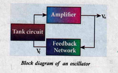
An oscillator circuit consists of three components.
(i) Tank circuit
(ii) Amplifier
(iii) feedback network
(i) Amplifier:
(a) This is a single stage amplifier which amplifies the weak signal produced by the tank circuit.
(b) The required output is supplied by this amplifier.
(ii) Feedback (network):
(a) The circuit used to feedback a portion of the ouput to the input is called the feedback network.
(b) If the portion of the output fed to the input is in phase with the input then the magnitude of the input signal increases.
(c) This process is called positive feedback which is necessary for sustained oscillations.
(iii) Tank Circuit:
.jpg)
(a) It consists of an inductance (L) and a capacitor (C) connected in parallel as shown in figure.
(b) Whenever energy is supplied to the tank circuit from a dc source, the energy is stored in inductor and capacitor alternatively.
(c) This produces electrical oscillations of definite frequency.
(iv) Working :
(a) The tank circuit generates electrical oscillations and acts as the AC input source to the transistor amplifier. Amplifier amplifies the input AC signal. In practical oscillator circuits, there is loss of some energy in inductor coils and capacitors due to electrical resistance. A small amount of energy is used up in overcoming these losses during every cycle of
charging and discharging of the capacitor. Due to this, the amplitude of the oscillations decreases gradually. Hence, the tank circuit produces damped electrical oscillations.
(ii) In order to produce undamped oscillations, a positive feedback is provided from output to input by feedback network. This Compensates encrgy loss in tank circuit. The frequency oscillations is deternined by the values of L and C and is given by \(f=\frac{1}{2 \pi \sqrt{L C}}\)
5.
(i) The satellite communication is a mode of transmission of signal between transmitter and receiver via satellite.
(ii) The message signal from the Earth station is transmitted to the satellite on board via an uplink (frequency band 6 GHz), amplified by a transponder and then retransmitted to another earth station via a downlink (frequency band 4 GHz).
Applications:
Satellites are classified into different types based on their applications.
(i) Weather Satellites:
They are used to monitor the weather and climate of Earth. By measuring cloud mass, these satellites enable us to predict rain and dangerous storms like hurricanes, cyclones etc.
(ii) Communication satellites:
They are used to transmit television, radio, internet signals etc. Multiple satellites are used for long distance communication
(iii) Navigation satellites:
These are employed to determine the geographic location of ships, aircraft or any other object.
6.
(i) It is used for personal communication and cellular phones offer voice and data connectivity with high speed.
(ii) Transmission of news across the globe is done within a few seconds.
(iii) Using Internet of Things (UIT), it is made possible to control various devices from a single device. Example: home automation using a mobile phone.
(iv) It enables smart classrooms, online availability of notes, monitoring student activities etc. in the field of education.
7.
(i) Radar basically stands for Radio Detection and Ranging System.
(ii) It is one of the important applications of communication systems' and is mainly used to sense, detect, and locate distant objects like aircraft, ships, spacecraft, etc.
(iii) The angle, range, or velocity of the objects that are invisible to the human eye can be determined.
(iii) Radar uses electromagnetic waves for communication. The electromagnetic signal is initially radiated into space by an antenna in all directions.
(iv) When this signal strikes the targeted object, it gets reflected or reradiated in many directions.
(v) This reflected (echo) signal is received by the radar antenna which in turn is delivered to the receiver.
(vi) Then, it is processed and amplified to determine the geographical statistics of the object. The range is determined by calculating the time taken by the signal to travel from RADAR to the target and back.
Applications :
Radars find extensive applications in almost all fields.
(i) In military, it is used for locating and detecting the targets.
(ii) It is used in navigation systems such as ship borne surface search, air search and weapons guidance systems.
(iii) To measure precipitation .rate and wind speed in meteorological observations, Radars are used.
(iv) It is employed to locate and rescue people in emergency situations.
8.
VBE =0.7V
Input junction is a forward biased.
Since,
VBE = 0.7V
VCE = VBE+ VCB
VCB = VCE-VBE
To determine VCB we find IC
\({ I }_{ C }\cong { I }_{ C }\frac { 2-{ V }_{ BE } }{ { R }_{ 2 } } =\frac { 2-0.7 }{ 1k\Omega } \)
IC = 1.3mA
VCE = VCC - IC (R1 + R2)
= 10 - 1.3mA (10K + 1K)
VCE = - 4.3 V
VCE =-4.3V-0.7
VCB = - 5V
9.
α = 0.98
ICu = 0.6 μA
\(\alpha =\frac { \beta }{ 1+\beta } \)
(or)
\(0.98=\frac { 1 }{ \frac { 1 }{ \beta } +1 } \)
β = 49
ICEO = (1 + β)ICBO
= (1 + 49) x 0.6μA
ICEO = 30 μA
= (1 + 49) x 0.6 μA
ICEO = 30 μA
IC = βIB+ ICEO
= 49 x 20 μA + 30 μA
IC = 1.01 mA
10.
Insulators:
(i) The valence band and the conduction band are separated by a large energy gap.
(ii) The forbidden energy gap is approximately 6 eV in insulators.
(iii) The gap is very large that electrons from valence band cannot move into conduction band even on the application of strong external electric field or the increase in temperature.
Metals
(i) In metals, the valence band and conduction band overlap.
(ii) Hence, electrons can move freely into the conduction band which results in a large number of free electrons in the conduction band.
Semiconductors
(i) In semiconductors, there exists a narrow forbidden energy gap (E < 3eV) between - g the valence band and the conduction band.
(ii) Free electrons are small in number, the conductivity of the semiconductors is not as high as that of the conductors.
11.
(i) This gives the variation of collector current (IC) with changes in base current (IB) at constant collector-emitter voltage (VCE).
(ii) It is seen that a small Ie flows even when IB is zero. This current is called the common emitter leakage current (ICEQ) which is due to the flow of minority charge carriers.
Forward current gain:
(i) The ratio of the change in collector current (ΔIC) to the change in base current (ΔIB) at constant collector-emitter voltage (VCE) is called forward current gain(β)
\(\beta ={ \left( \frac { \triangle { I }_{ C } }{ \triangle { I }_{ B } } \right) }_{ { V }_{ CE } }\)
(ii) It is value is very high and it generally ranges from 50 to 200. It depends on the construction of the transistors and will be provided by the manufacturer.
12.
(i) An oscillator basically converts de energy into ac energy of high frequency ranging from a few Hz to several MHz.
(ii) There are two types of oscillators
a) Sinusoidal
b) Non-sinusoidal.
(iii) Sinusoidal oscillators generate oscillations in the form of sine wave at constant amplitude and frequency.
(iv) Non-sinusoidal oscillators generate complex non-sinusoidal waveforms like square wave, Triangular - wave or Sawtooth -wave
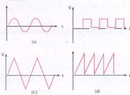
(v) Sinusoidal oscillations can be of two types:
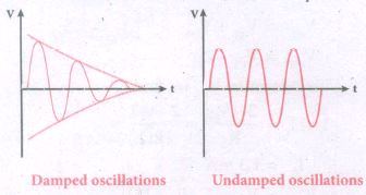
a) Damped
b) undamped.
(vi) If the amplitude of the electrical oscillations decreases with time due to energy loss, is called damped oscillations
(vii) The amplitude of the electrical oscillations remains constant with time in undamped oscillations.
13.
Insulators
(i) The gap is very large that electrons from valence band cannot move into conduction band even on the application of strong external electric field or the increase in temperature.
(ii) The electrical conduction is not possible as the free electrons are almost nil.
(iii) Its resistivity is in the range of 1011 - 1019 Ωm
Metals
(i) Conduction becomes possible even at low temperatures.
(ii) The application of electric field provides sufficient energy to the electrons to drift in a particular' direction to constitute a current.
(iii) The resistivity value lies between 10-2 and 10-8Ωm
Semiconductors
(i) At a finite temperature, thermal agitations in the solid can break the covalent bond between the atoms.
(ii) This releases some electrons from valence band to conduction band
(iii) The resistivity value of semiconductors is from 10-5 to 10-6 Ωm
(iv) When the temperature is increased further, more number of electrons is promoted to the conduction band and increases the conduction.
(v) Thus, electrical conduction increases with the increase in temperature.

12th Standard Syllabus & Materials
12th Standard
TN 12th Computer Applications களப்பெயர் முறைமை (DNS) Sample Question Papers Study Material - QB365 Set A
NEW12th Standard
TN 12th Computer Applications வலையமைப்பு எடுத்துக்காட்டுகள் மற்றும் நெறிமுறைகள் Sample Question Papers Study Material - QB365 Set A
NEW12th Standard
TN 12th Computer Applications கணினி வலையமைப்பு ஓர் அறிமுகம் Sample Question Papers Study Material - QB365 Set A
NEW12th Standard
TN 12th Computer Applications PHP-உடன் MySQL-ஐ இணைத்தல் Sample Question Papers Study Material - QB365 Set A



Tamilnadu Stateboard 12th Standard Subjects

Maths

Chemistry
Physics

Biology

Computer Science

Business Maths and Statistics

Economics

Commerce

Accountancy

History

Computer Applications
Biology
Computer Technology
Computer Applications
Computer Science
Business Maths and Statistics
Commerce
Economics
Maths
Chemistry
Physics
Computer Technology
History
Accountancy

Tamil

English

French
Tamilnadu Stateboard Standards

