
 100% FREE ACCESS
12th Standard Syllabus & Materials
12th Standard
TN 12th Computer Applications மின்னணு தரவு பரிமாற்றம் Sample Question Papers Study Material - QB365 Set A
NEW12th Standard
TN 12th Computer Applications மின் - வணிக பாதுகாப்பு அமைப்புகள் Sample Question Papers Study Material - QB365 Set A
NEW12th Standard
TN 12th Computer Applications மின்னணு செலுத்தல் முறைகள் Sample Question Papers Study Material - QB365 Set A
NEW12th Standard
TN 12th Computer Applications மின் - வணிகம் Sample Question Papers Study Material - QB365 Set A
NEW12th Standard
TN 12th Computer Applications திறந்த மூல கருத்துருக்கள் Sample Question Papers Study Material - QB365 Set A
NEW12th Standard
TN 12th Computer Applications வலையமைப்பு வடமிடல் Sample Question Papers Study Material - QB365 Set A

Published on: 27/01/2021
12th Standard Physics English Medium Electronics and Communication Systems Reduced Syllabus Important Questions 2021
Download Tamil Nadu 12th Standard Physics question papers, model tests, one-mark questions, important questions, and public exam papers in PDF format. Free study materials and answer keys for TN State Board students.
Questions + Answers key
Take MCQ Physics Test1.
Output characteristics of an NPN, transistor in CE mode is drawn between ___________
IC and VBE
IE and VCE
IB and VCE
IC and VCE
2.
ln NPN transistors, when the emitter-base junction is forward-biased, the direction of conventional current is from _____________
base to emitter
emitter to base
collector to base
base to collector
3.
In PNP transistors, the direction of conventional current, when emitter-base junction is forward-biased is from __________
base to emitter
emitter to base
collector to base
base to collector
4.
To remove d.c. voltage fluctuations we use _______
filter circuits
sieve circuits
conductor circuits
rectifier circuits
5.
Doped semiconductors are ____________
extrinsic
intrinsic
simple
charged
6.
Pure semiconductors are called _________
extrinsic semiconductor
intrinsic semiconductor
simple semiconductor
charged semiconductor
7.
Resistance of a semiconductor is ______ to temperature change.
directly proportional
indirectly proportional.
a constant
independent
8.
If the distance between the conduction band and valence band is leV, then this combination is _______________.
semiconductor
metal
insulator
conductor
9.
The energy band gap is maximum in ________________.
metals
insulators
semiconductor
superconductors
10.
The radiation of electrical energy is practicable only above _________
20 kHz
200 MHz
200 kHz
20 Hz
11.
To obtain a p-type germanium semiconductor, it must be doped with _____________.
Indium
phosphorus
arsenic
antimony
12.
From the follwoing semi-conductor devices _________ operates in forward bias only.
varactar diode
zener diode
light emitting diode
photo-diode
13.
In an N-P-N transistor circuit, the emitter, collector, and base current are respectively IE, IC, and lB. The relation between them is _____________.
IC
IB
IB > IC > IE
IB > IC > IE
14.
Which of the following is not the advantage of PN junction diode over tube value?
Unlimited life
No warming-up time after switching
Large efficiency
Low consumption of power
15.
The output transducer of the communication system converts the radio signal into ________.
Sound
Mechanical energy
Kinetic energy
None of the above
16.
What is mobile communication?
17.
Write the demerits of fiber optic communication?
18.
Define Zener effect
19.
Define Reverse bias.
20.
Define energy band
21.
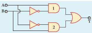
In the combination of the following gates, write the Boolean equation for output Y in terms of inputs A and B.
22.
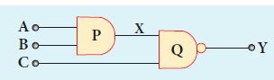
What is the output Y in the following circuit, when all the three inputs A, B, and C are first 0 and then 1?
23.
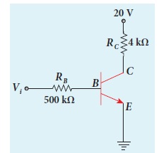
In the circuit shown in the figure, the input voltage Vi is 20 V, VBE = 0 V, and VCE = 0 V. What are the values of IB, IC, β?
24.
Determine the wavelength of light emitted from LED which is made up of GaAsP semiconductor whose forbidden energy gap is 1.875 eV. Mention the colour of the light emitted (Take h = 6.6 x 10⁻³⁴ Js).
25.
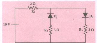
The given circuit has two ideal diodes connected as shown in figure below. Calculate the current flowing through the resistance R1.
26.
What is the phase relationship between the AC input and output voltages in a common emitter amplifier? What is the reason for the phase reversal?
27.
28.
Define electron motion in a semiconductor.
29.
Why ground wave cannot be used for long distance communication using high frequency?
30.
What are the application of satellite communication?
31.
What are the advantages of FM
32.
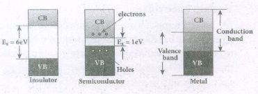
Give the Schematic representation of valence band, conduction band, and forbidden energy gap and draw energy band structure of
(a) Insulators
(b) Semiconductors
(c) Metals?
33.
Calculate the range of the variable capacitor that is to be used in a tuned-collector oscillator which has a fixed inductance of 150 μH. The frequency band is from 500 kHz to 1500 kHz.
34.
Write a note on photodiode.
35.
Discuss the biasing polarities in an NPN and PNP transistors
36.
Write the applications of mobile communication.
37.
Write any two distinguishing features between Insulators, Metals and semiconductors and insulators an the basis of energy band diagrams.
38.
Explain and classify transistor as an oscillator.
39.
State and prove De Morgan’s first and second theorem.
40.
State Boolean laws. Elucidate how they are used to simplify Boolean expressions with suitable example.
41.
Explain the formation of depletion region and barrier potential in PN junction diode.
42.
Elucidate the formation of a N -type and P-type semiconductors.
43.
Give circuit symbol, logical operation, truth table, and Boolean expression of
i) AND gate
ii) OR gate
iii) NOT gate
iv) NAND gate
v) NOR gate and
vi) EX-OR gate.
1.
(a)
IC and VBE
2.
(a)
base to emitter
3.
(b)
emitter to base
4.
(a)
filter circuits
5.
(a)
extrinsic
6.
(b)
intrinsic semiconductor
7.
(b)
indirectly proportional.
8.
(a)
semiconductor
9.
(c)
semiconductor
10.
(a)
20 kHz
11.
(a)
Indium
12.
(c)
light emitting diode
13.
(b)
IB
14.
(a)
Unlimited life
15.
(a)
Sound
16.
Mobile communication is used to communicate with others in different locations without the use of any physical connection like wires or cables.
17.
(i) Fiber optic cables are more fragile when compared to copper wires.
(ii) It is an expensive technology.
18.
Electric field is strong enough to break (or) rep tune the covalent bonds in the lattice and there by generating electron - hole pairs. This effect is called Zener effect.
19.
If the positive terminal battery is conneted to the n-side and the negative potential to the p-side, the junction is said to be reverse biased.
20.
Band of very large number of closely spaced energy levels in a very small energy range is known as energy band.
21.
The output at the 1st AND gate : A\(\overline { B } \)
The output at the 2nd AND gate : ĀB
The output at the OR gate: Y = A. \(\overline { B } \) + Ā .B
22.
| A | B | C | X = A.B | Y=\(\overline { X.C } \) |
| 0 | 0 | 0 | 0 | 1 |
| 1 | 1 | 1 | 1 | 0 |
23.
\({ I }_{ B }=\frac { { V }_{ i } }{ { R }_{ B } } =\frac { 20V }{ 500k\Omega } =40\mu A\) [∵ VBE = 0V]
\({ I }_{ C }=\frac { { V }_{ CC } }{ { R }_{ C } } =\frac { 20V }{ 4k\Omega } =5mA\) [∵ VCE = 0V]
\(\beta =\frac { { I }_{ C } }{ { I }_{ B } } =\frac { 5mA }{ 40\mu A } =125\)
24.
\({ E }_{ g }=\frac { hc }{ \lambda } \)
Therefore,
\(\lambda =\frac { hc }{ { E }_{ g } } =\frac { 6.6\times { 10 }^{ -34 }\times 3\times { 10 }^{ 8 } }{ 1.875\times 1.6\times { 10 }^{ -19 } } \)
= 660 nm
The wavelength 660 nm corresponds to red colour light
25.
V= 10V, R1 = 2 Ω, R3 = 2 Ω
Diode D1 is reverse biased so it will block the current and diode D2 is forward biased, so it will pass the current.
\(\mathrm{R} =\mathrm{R}_{1}+\mathrm{R}_{2} \)
\(=2+2=4 \Omega \)
\(\mathrm{I} =\frac{\mathrm{V}}{\mathrm{R}}=\frac{10}{4} \)
I = 2.5 A
26.
(i) The output signal is reversed by 180o. During the positive half cycle, Input signal (Vs) increases the forward voltage across the emitter-base.
(ii) As a resultthe base current (IB) increases. Consequently, the collector current (IC) increases ß times.
(iii) This increases the voltage drop across Rc (IC RC) which in turn decreases the collector-emitter voltage (VCE).
(iv) Therefore, the input signal in the positive direction produces an amplified signal in the negative direction at the output.
27.
28.
(i) To move the hole in a given direction, the valence electrons move in the opposite direction.
(ii) Electrons flow in a N-type semiconductor is similar to electrons moving in a metallic wire.
(iii) The N- type dopant atoms will yield electrons available for conduction.
29.
The maximum range of propagation in this mode depends on
(i) transmitted power and
(ii) frequency (less than a few MHz) of high frequencies the rate of energy dissipation of the signal increases and the signal gets attenuated over a short distance.
30.
i) Weather Satellites : They are used to monitor the weather and climate of Earth. By measuring cloud mass, these satellites enable us to predict rain and dangerous storms like hurricanes, cyclones, etc.
ii) Navigation satellites : These are employed to determine the geographic location of ships, aircraft or any other object.
iii) Communication satellites: Thev are used to transmit television, radio, internet signals etc. Multiple satellites are used for long distance communication.
31.
i) Large decrease in noise. This leads to an increase in signal-noise ratio.
ii) The operating range is quite large.
iii) The transmission efficiency is very high as all the transmitted power is useful.
iv) FM bandwidth covers the entire frequency range which humans can hear. Due to this, FM radio has better quality compared to AM radio.
32.
33.
Resonant frequency, \({ f }=\frac { 1 }{ 2\pi \sqrt { LC } } \)
On simplifying, we get C = \(\frac { 1 }{ { 4\pi }^{ 2 }{ { f }^{ 2 } }L } \)
i) When frequency = 500 kHz,
\(C=\frac { 1 }{ 4\times { 3.14 }^{ 2 }\times { (500\times { 10 }^{ 3 }) }^{ 2 }\times 150\times { 10 }^{ -6 } } \)
= 676 pF
ii) When frequency = 1500 kHz,
\(C=\frac { 1 }{ 4\times { 3.14 }^{ 2 }\times { (1500\times { 10 }^{ 3 }) }^{ 2 }\times 150\times { 10 }^{ -6 } } \)
= 75 pF
Therefore, the capacitor range is 75 to 676 pF.
34.
Photo diode:
A p -n junction diode which converts an optical signal into electrical current is known as photodiode.
(i) The operation of photodiode is exactly inverse to that of an LED. Photodiode works in reverse bias condition.
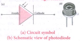
(ii) The direction of arrows indicates that the light is incident on the photo diode.
(iii) The device consists of a p-n junction semiconductor made of photosensitive material kept safely inside a plastic case as shown in fig.
(iv) It has a small transparent window that allows light to be incident on the p-n junction.
(v) Photodiodes car generate current when the p - n junction is exposed to light and hence are called as light sensors.
(vi) When a photon of sufficient energy (hv) strikes the depletion region of the diode, some of the valence band electron are elevated into conduction band, in turn holes are developed in the valence band. This creates electron-hole pairs. The amount of electron - hole pairs generated depends on the intensity of light incident on the p - n junction.
(vii) These electron and holes are swept across the p-n junction by the electric field created by reverse voltage before recombination takes place. Thus, holes move towards the n - side and electrons towards the P - side - when the external circuit is made, the electrons flow through the external circuit and constitute the photo current.
(viii) When the incident light is zero, there exists a reverse current which is negligible. This reverse current in the absence of any. incident light is called dark current and is. due to the thermally generated minority carriers.
35.
(i) In NPN transistor, a positive voltage is given to the collector terminal to produce a current flow from the collector to the emitter.
(ii) In a PNP transistor, a positive voltage is given to the emitter terminal to produce current flow from the emitter to collector.
(iii) To operate the transistor in the active region, emitter-base must be forward biased and collector base must be reverse biased.
36.
(i) It is used for personal communication and cellular phones offer voice and data connectivity with high speed.
(ii) Transmission of news across the globe is done within a few seconds.
(iii) Using Internet of Things (UIT), it is made possible to control various devices from a single device. Example: home automation using a mobile phone.
(iv) It enables smart classrooms, online availability of notes, monitoring student activities etc. in the field of education.
37.
Insulators:
(i) The valence band and the conduction band are separated by a large energy gap.
(ii) The forbidden energy gap is approximately 6 eV in insulators.
(iii) The gap is very large that electrons from valence band cannot move into conduction band even on the application of strong external electric field or the increase in temperature.
Metals
(i) In metals, the valence band and conduction band overlap.
(ii) Hence, electrons can move freely into the conduction band which results in a large number of free electrons in the conduction band.
Semiconductors
(i) In semiconductors, there exists a narrow forbidden energy gap (E < 3eV) between - g the valence band and the conduction band.
(ii) Free electrons are small in number, the conductivity of the semiconductors is not as high as that of the conductors.
38.
(i) An oscillator basically converts de energy into ac energy of high frequency ranging from a few Hz to several MHz.
(ii) There are two types of oscillators
a) Sinusoidal
b) Non-sinusoidal.
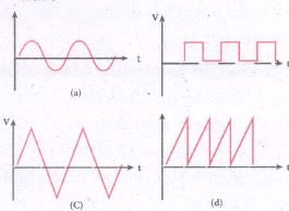
(iii) Sinusoidal oscillators generate oscillations in the form of sine wave at constant amplitude and frequency.
(iv) Non-sinusoidal oscillators generate complex non-sinusoidal waveforms like square wave, Triangular - wave or Sawtooth -wave
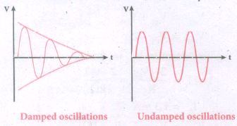
(v) Sinusoidal oscillations can be of two types:
a) Damped
b) undamped.
(vi) If the amplitude of the electrical oscillations decreases with time due to energy loss, is called damped oscillations
(vii) The amplitude of the electrical oscillations remains constant with time in undamped oscillations.
39.
First Theorem :
The complement of the sum of two logical inputs is equal to the product of its complements.
\(\overline { A+B } \) = \(\bar { A } .\bar { B } \)
Proof:
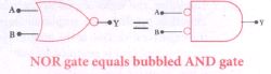
(i) The Boolean equation for NOR gate is Y = \(\overline { A+B } \)
(ii) The Boolean equation for a bubbled AND gate is Y =\(\bar { A } .\bar { B } \)
(iii) Both cases generate same outputs for same inputs. It can be verified using the following truth
| A | B | A+B | \(\overline { A+B } \) | Ā | \(\bar { B } \) | \(\bar { A } .\bar { B } \) |
| 0 | 0 | 0 | 1 | 1 | 1 | 1 |
| 0 | 1 | 1 | 0 | 1 | 0 | 0 |
| 1 | 0 | 1 | 0 | 1 | 0 | 0 |
| 1 | 1 | 1 | 0 | 0 | 0 | 0 |
(i) From the above truth table, we can conclude \(\overline { A+B } \) = \(\bar { A } .\bar { B } \)
(ii) Thus De Morgan's first theorem is proved.
(iii) Hence, a NOR gate is equal to a bubbled AND gate
Second theorem :
The complement of the product of two is equal to the sum of its complements
\(\overline { A.B } \) = \(\bar { A } +\bar { B } \)
Proof:
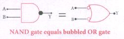
(i) The Boolean equation for NAND gate is Y = \(\overline { A.B } \)
(ii) The Boolean equation for bubbled OR gate is Y = \(\bar { A } +\bar { B } \)
(iii) A and B are the inputs and Y is the output. The above two equations produces the same output for the same inputs. It can be verified by using the truth table.
| A | B | A+B | \(\overline{\mathrm{A}. \mathrm{B}}\) | Ā | \(\bar { B } \) | \(\overline{\mathrm{A}}+\overline{\mathrm{B}}\) |
| 0 | 0 | 0 | 1 | 1 | 1 | 1 |
| 0 | 1 | 0 | 1 | 1 | 0 | 1 |
| 1 | 0 | 0 | 1 | 0 | 1 | 1 |
| 1 | 1 | 1 | 0 | 0 | 0 | 0 |
(i) From the above truth table, we can conclude \(\overline { A.B } \) = \(\bar { A } +\bar { B } \)
(ii) Thus, De Morgan's second therom is proved.
(iii) Hence, a NAND gate is equal to a bubbled OR gate.
40.
Laws of Boolean algebra:
Complement law:
| A | Y=Ā |
| 0 | Y = \(\bar { 0 } \) = 1 |
| 0 | Y=\(\bar { 1 } \)=0 |
The complement law can be realised as Ā = A
OR laws:
| A | B | Y=A+B |
| 0 | 0 | Y = 0 + 0 = 0 |
| 0 | 1 | Y = 0 + 1 = 1 |
| 1 | 0 | Y = 1 + 0 = 1 |
| 1 | 1 | Y = 1 + 1 = 1 |
The OR laws can be realised as:
| 1st law | A+0=A |
| 2st law | A+1=1 |
| 3st law | A+A=A |
| 4st law | A+Ā=1 |
AND law:
| A | B | Y=A.B |
| 0 | 0 | Y=0.0=0 |
| 0 | 1 | Y=0.1=0 |
| 1 | 0 | Y=1.0=0 |
| 1 | 1 | Y=1.1=1 |
The AND laws can be realised as:
| 1st law | A.0=0 |
| 2st law | A.1=A |
| 3st law | A.A=A |
| 4st law | A.Ā=0 |
The Boolean operations obey the folloWing laws:
Communtative laws:
A+B =B+A
A.B =B.A
A sociate laws:
A + (B + C) = (A + B) + C
A. (B.C) = (A.B).C
D stributive laws:
A (B + C) = AB + BC
A + BC = (A + B) (A + C)
The above laws are used to simplify complicated expressions and to simplify the logic circuitry.
41.
i) Formation of depletion layer
(i) A single piece of semiconductor crystal is suitably doped such that its one side is p-type semiconductor and the other side is n-type semiconductor.
(ii) The contact surface between the two sides is called p-n junction. Whenever p-n junction is formed, some of the free electrons diffuse from the n-side to the p-side while the holes from the P-Side to the n-side.
(iii) The diffusion of charge carriers happens due to the fact that the n-side has higher electron concentration and the p-side has higher hole concentration.
(iv) The diffusion of the majority charge carriers across the junction gives rise to an electric current, called diffusion current.
(v) When an electron leaves the n-side, a pentavalent atom in the n-side becomes a positive ion.
(vi) The free electron migrating into p-side recombines with a hole present in a trivalent atom near the junction and the trivalent atom becomes a negative ion. Since such ions are bonded to the neighbouring atoms in the crystal lattice, they are unable to move.
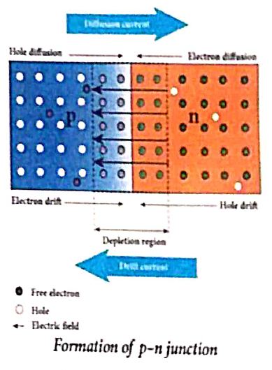
(vii) As the diffusion process continues, a laver of positive ions and a layer of negative ions are created on either side of the junction accordingly.
(viii) The thin region near the junction which is free from charge carriers (free electrons and holes) is called depletion region.
(ix) An electric field is set up between the positively charged layer in the n-side and the negatively charged layer in the p-side in the depletion region.
(x) This electric field makes electrons in the p-side drift into the n-side and the holes in the n-side into the p-side.
(xi) The electric current produced due to the motion of the minority charge carriers by the electric field is known as drift current. The diffusion current and drift current flow in opposite directions.
(xii) Though drift current is less than diffusion current initially, equilibrium is reached between them at a particular time.
(xiii) With each electron (or hole) diffusing across the junction, the strength of the electric field increases thereby increasing the drift current till the two currents become equal
(xiv)Hence at equilibrium, there is no net electric current across the junction. Thus, a p-n junction is formed.
ii) Junction potential or barrier potential
.JPG)
(i) The movement of charge carriers across the junction takes place only to a certain point beyond which the depletion layer acts like a barrier to further diffusion of free charges across the junction.
(ii) This is due to the fact that the immobile ions on both sides establish an electric potential difference across the junction.
(iii) Therefore, an electron trying to diffuse into the interior of the depletion region encounters a wall of negative ions repelling it backwards.
(iv) If the free electron has enough energy, it can break through the wall and enter into the p-region, where it can recombine with a hole and create another negative ion.
(v) The strength of the electric potential difference across the depletion region keeps on increasing with the crossing of each electron until equilibrium is reached, at this point, the internal repulsion of the depletion layer stops further diffusion of free electrons across the junction.
(vi) The difference in potential across the depletion layer is called the barrier potential (Vb).
(vii) At 25°C, this barrier potential is approximately 0.7 V for silicon and 0.3 V for germanium.
42.
n-type semiconductor:
(i) A n-type semiconductor is obtained by doping a pure Germanium (or Silicon) crystal with a dopant from group V pentavalent elements like Phosphorus, Arsenic, and Antimony.
(ii) The dopant has five valence electrons while the Germanium atom has four valence electrons.
(iii) During the process of doping, a few of the Germanium atoms are replaced by the group V dopants.
(iv) Four of the five valence electrons of the impurity atom are bound with the 4 valence electrons of the neighbouring replaced Germanium atom
(v) The fifth valence electron of the impurity atom will be loosely attached with the nucleus as it has not formed the covalent bond.
(vi) The energy level of the loosely attached fifth electron from the dopant is found just below the conduction band edge and is called the donor energy level.
(vii) At room temperature, these electrons can easily move to the conduction band with the absorption of thermal energy
(viii) Besides, an external electric field also can set free the loosely bound electrons and lead to conduction.
(ix) It is important to note that the energy required for an electron to jump from the valence band to the conduction band (Ee ) g in an intrinsic semiconductor is 0.7 eV for Ge and 1.1 eV for Si, while the energy required to set free a donor electron is only 0.01 eV for Ge and 0.05 eV for Si.
(x) The group V pentavalent impurity atorns. donate electrons to the conduction band and are called donor impurities. Therefore, each impurity atom provides one extra electron to the conduction band in addition to the thermally generated electrons.
(xi) These electrons leave holes in the valence band. Hence, the majority carriers of current in an n-type semiconductor are electrons and the minority carriers are holes. Such a semiconductor doped with a pentavalent impurity is called an n-type semiconductor.
p-type semiconductor:
(i) A trivalent atom from group III elements such as Boron, Aluminium, Gallium and Indium is added to the Germanium or Silicon substrate. The dopant with three valence electrons is bound with the neighbouring Germanium atom.
(ii) As Germanium atom has four valence electrons, one electron position of the dopant in the Germanium crystal lattice will remain vacant. The missing electron position in the covalent bond is denoted as a hole.
(iii) To make complete covalent bonding with all four neighbouring atoms, the dopant is in need of one more electron
(iv) These dopants can accept electrons from the neighbouring atoms. Therefore, this impurity is called an acceptor impurity The energy level of the hole created by each impurity atom is just above the valence band and is called the acceptor energy level band and is called the acceptor energy level.
(v) For each acceptor atom, there will be a hole in the valence band in addition to the thermally generated holes. In such an extrinsic semiconductor, holes are the majority carriers and thermally generated electrons are minority carriers. The semiconductor thus formed is called a p-type semiconductor.
43.
i) AND gate
a) Circuit Symbol:
The circuit symbol of a two input AND gate is shown in Figure (a). A and B are inputs and Y is the output. It is a logic gate and hence A, B, and Y can have the value of either 1 or 0
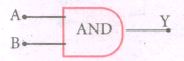
Two input AND gate
| Inputs | outputs | |
| A | B | Y = A + B |
| 0 | 0 | 0 |
| 0 | 1 | 0 |
| 1 | 0 | 0 |
| 1 | 1 | 1 |
Truth table
b) Boolean equation:
Y = A.B
It performs logical multiplication and is different from arithmetic multiplication.
c) Logic operation:
The output of AND gate is high only when all the inputs are high. In the rest of the cases, the output is low. It is represented in the truth table (Figure (b).
ii) OR gate
a) Circuit Symbol:
The circuit symbol of a two input OR gate is shown in Figure (a). A and B are inputs and Y is the output.
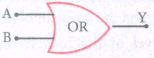
The input OR gate
| Inputs | outputs | |
| A | B | Y = A + B |
| 0 | 0 | 0 |
| 0 | 1 | 1 |
| 1 | 0 | 1 |
| 1 | 1 | 1 |
Truth table
a) Boolean equation:
A + B = Y
It performs logical addition and is different from arithmetic addition.
b) Logic operation:
The output of OR gate is high (logic 1 state) when either of the inputs or both are high. The truth table of OR gate is shown in Figure (a).
iii) NOT gate
a) Circuit Symbol:
The circuit symbol of NOT gate is shown in Figure (a). A and B are inputs and Y is the output.
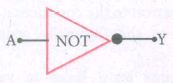
NOT gate
| Inputs | Output |
| A | Y = Ā |
| 0 | 1 |
| 1 | 0 |
Truth table
a) Boolean equation:
Y = Ā
b) Logic operation:
The output is the complement of the input. It is represented with an overbar. It is also called as inverter. The truth table infers that the output Y is I when input A is 0 and vice versa. The truth table of NOT is shown in Figure (b).
iv) NAND gate
a) Circuit Symbol:
The circuit symbol of NAND gate is shown in Figure (a). A and B are inputs and Y is the output.

Two input NAND gate
| Inputs | Output (AND) |
outputs (NAND) |
|
| A | B | Z = A.B | Y = \(\overline { A.B } \) |
| 0 | 0 | 0 | 1 |
| 0 | 1 | 0 | 1 |
| 1 | 0 | 0 | 1 |
| 1 | 1 | 1 | 0 |
Truth table
b) Boolean equation:
Y = \(\overline { A.B } \)
Logic operation:
The output Y equals, the complement of AND operation. The circuit is an AND gate followed by a NOT gate. Therefore, it is summarized as NAND. The output is at logic zero only when all the inputs are high. The rest of the cases, the output is high (Logic I state). The truth table of NAND gate is shown in Figure (b).
v) NOR gate
a) Circuit Symbol:
The circuit symbol of NOR gate is shown in Figure (a). A and B are inputs and Y is the output.

Two input NANS gate
| Inputs | Output (OR) |
outputs (NOR) |
|
| A | B | Z = A + B | Y = \(\overline { A+B } \) |
| 0 | 0 | 0 | 1 |
| 0 | 1 | 1 | 0 |
| 1 | 0 | 1 | 0 |
| 1 | 1 | 1 | 0 |
Truth table
Boolean equation:
Y = \(\overline { A+B } \)
Logic operation:
The output Y equals the complement of OR operation (A OR B). The circuit is an OR gate followed by a NOT gate and is summarized as NOR. The output is high when all the inputs are low. The output is low for all other combinations of inputs. The truth table of NOR gate is shown in Figure (b).
vi) Ex-OR gate
a) Circuit Symbol:
The circuit symbol of Ex-OR gate is shown in Figure (a). A and B are inputs and Y is the output. The Ex-OR operation is denoted as ⊕
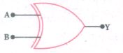
Ex-OR gate
| Inputs | outputs (Ex-OR) |
|
| A | B | Y = A ⊕ B |
| 0 | 0 | 0 |
| 0 | 1 | 1 |
| 1 | 0 | 1 |
| 1 | 1 | 0 |
Truth table
b) Boolean equation
Y = \(A.\overline { B } \) + \(\overline { A }.B \)
Y = A ⊕ B
Logic operation:
The output is high only when either of the two inputs is high. In the case of an Ex-OR gate with more than two inputs, the output will be high when odd number of inputs are high. The truth table of Ex-OR gate is shown in Figure (b).

12th Standard Syllabus & Materials
12th Standard
TN 12th Computer Applications களப்பெயர் முறைமை (DNS) Sample Question Papers Study Material - QB365 Set A
NEW12th Standard
TN 12th Computer Applications வலையமைப்பு எடுத்துக்காட்டுகள் மற்றும் நெறிமுறைகள் Sample Question Papers Study Material - QB365 Set A
NEW12th Standard
TN 12th Computer Applications கணினி வலையமைப்பு ஓர் அறிமுகம் Sample Question Papers Study Material - QB365 Set A
NEW12th Standard
TN 12th Computer Applications PHP-உடன் MySQL-ஐ இணைத்தல் Sample Question Papers Study Material - QB365 Set A



Tamilnadu Stateboard 12th Standard Subjects

Maths

Chemistry
Physics

Biology

Computer Science

Business Maths and Statistics

Economics

Commerce

Accountancy

History

Computer Applications
Biology
Computer Technology
Computer Applications
Computer Science
Business Maths and Statistics
Commerce
Economics
Maths
Chemistry
Physics
Computer Technology
History
Accountancy

Tamil

English

French
Tamilnadu Stateboard Standards

