
 100% FREE ACCESS
12th Standard Syllabus & Materials
12th Standard
TN 12th Computer Applications மின்னணு தரவு பரிமாற்றம் Sample Question Papers Study Material - QB365 Set A
NEW12th Standard
TN 12th Computer Applications மின் - வணிக பாதுகாப்பு அமைப்புகள் Sample Question Papers Study Material - QB365 Set A
NEW12th Standard
TN 12th Computer Applications மின்னணு செலுத்தல் முறைகள் Sample Question Papers Study Material - QB365 Set A
NEW12th Standard
TN 12th Computer Applications மின் - வணிகம் Sample Question Papers Study Material - QB365 Set A
NEW12th Standard
TN 12th Computer Applications திறந்த மூல கருத்துருக்கள் Sample Question Papers Study Material - QB365 Set A
NEW12th Standard
TN 12th Computer Applications வலையமைப்பு வடமிடல் Sample Question Papers Study Material - QB365 Set A

Published on: 27/01/2021
12th Standard Physics English Medium Electronics and Communication Systems Reduced Syllabus Important Questions With Answer Key 2021
Download Tamil Nadu 12th Standard Physics question papers, model tests, one-mark questions, important questions, and public exam papers in PDF format. Free study materials and answer keys for TN State Board students.
Questions + Answers key
Take MCQ Physics Test1.
The maximum carrier swing allowed in frequency modulation is ________________.
455 kHz
10.7 kHz
75 MHz
150 kHz
2.
The distance of a geostationary satellite's orbit from the Earth is about _______
366 km
108 km
36 x 103km
30 m
3.
________ wire is used between telephones and the central office
Flat
Multiconnector
Co-axial
Twisted pair
4.
_________ is the most often used wire material.
Copper
Aluminium
Sulphur
iron
5.
When the output is an complement of the input it is ____________
NOT gate
AND gate
OR
NAND
6.
Zener breakdown is mainly due to ________
collision
breaking of covalent bonds
doping
recombination
7.
Resistance of any photosensitive material is ______ to the intensity of light exposed
directly proportional
indirectly proportional
a constant
independent
8.
The speaker converts ________ energy into ______ energy.
electrical, sound
sound, electrical
light, sound
sound, mechanica
9.
Vacant energy levels are called _________
valence level
core level
conduction levels
compound level
10.
In an insulator the energy gap between the conduction band and valence band is of the order of _____________.
2MeV
5eV
1eV
10-3eV
11.
Microphone converts __________ energy into ________ energy.
sound, electrical
electrical, magnetic
magnetic, sound
light, heat
12.
The radiation of electrical energy is practicable only above _________
20 kHz
200 MHz
200 kHz
20 Hz
13.
The forbidden energy band gap in semi conductor, conductor and insulator are E1, E2 and E3 respectively. The relation among them is _______________.
E1. < E2 > E3
E1 > E2 > E3
E1 < E2 < E3
E1 > E2 < E3
14.
The output transducer of the communication system converts the radio signal into ________.
Sound
Mechanical energy
Kinetic energy
None of the above
15.
If a small amount of antimony (Sb) is added to germanium crystal,______.
it becomes a p-type semiconductor
the antimony becomes an acceptor atom
there will be more free electrons than hole in the semiconductor
its resistance is increased
16.
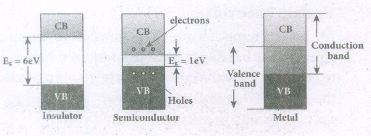
Give the Schematic representation of valence band, conduction band, and forbidden energy gap and draw energy band structure of
(a) Insulators
(b) Semiconductors
(c) Metals?
17.
Calculate the range of the variable capacitor that is to be used in a tuned-collector oscillator which has a fixed inductance of 150 μH. The frequency band is from 500 kHz to 1500 kHz.
18.
The output characteristics of a transistor connected in common emitter mode is shown in the figure. Determine the value of IC when VCE = 15 V. Also determine the value of IC when VCE is changed to 10 V
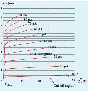
19.
A transistor having α = 0.99 and VBE = 0.7V, is connected in the common-cmiitter configuration as shown in figure. If the transister is in saturation region, find the value of the collector current.
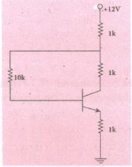
20.
Write a note on photodiode.
21.
Distinguish between wireline and wireless communication? Specify the range of electromagnetic waves in which it is used.
22.
Mention any three application Zener diode.
23.
Define Reverse bias.
24.
Define energy band
25.
In the circuit shown in the figure, the input voltage Vi is 20 V, VBE = 0 V, and VCE = 0 V. What are the values of IB, IC, β?
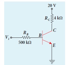
26.
Determine the wavelength of light emitted from LED which is made up of GaAsP semiconductor whose forbidden energy gap is 1.875 eV. Mention the colour of the light emitted (Take h = 6.6 x 10⁻³⁴ Js).
27.
A silicon diode is connected with 1kΩ resistor as shown. Find the value of current flowing through AB is
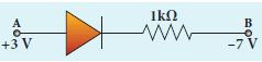
28.
Explain the current flow in a NPN transistor.
29.
Distinguish between avalanche breakdown and Zener breakdown.
30.
What do you mean by doping?
31.
32.
What does RADAR stand for?
33.
What is RADAR? Explain its function. State its applications
34.
For a BJT, the common - base current gain α = 0.98 and the collector base junction reverse bias saturation ICU = 0.6μA. This BJT is connected in the common emitter mode and operated in the active region with a base drive current ID= 20 μA. The collector current IC for this mode of operating is
35.
Write any two distinguishing features between Insulators, Metals and semiconductors and insulators an the basis of energy band diagrams.
36.
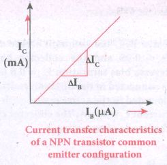
Explain current transfer characteristics.
37.
How does the change in temperature and application of electric field affect the behavior of materials and write the range of resistivity for each materials.
38.
Transistor functions as a switch. Explain.
39.
Draw the circuit diagram of a half-wave rectifier and explain its working.
40.
Give circuit symbol, logical operation, truth table, and Boolean expression of
i) AND gate
ii) OR gate
iii) NOT gate
iv) NAND gate
v) NOR gate and
vi) EX-OR gate.
41.
Fiber optic communication is gaining popularity among the various transmission media -justify.
42.
What do you know about GPS? Write a few applications of GPS.
43.
Explain the basic elements of communication system with the necessary block diagram.
1.
(d)
150 kHz
2.
(c)
36 x 103km
3.
(d)
Twisted pair
4.
(a)
Copper
5.
(d)
NAND
6.
(b)
breaking of covalent bonds
7.
(b)
indirectly proportional
8.
(a)
electrical, sound
9.
(c)
conduction levels
10.
(b)
5eV
11.
(a)
sound, electrical
12.
(a)
20 kHz
13.
(d)
E1 > E2 < E3
14.
(a)
Sound
15.
(c)
there will be more free electrons than hole in the semiconductor
16.
17.
Resonant frequency, \({ f }=\frac { 1 }{ 2\pi \sqrt { LC } } \)
On simplifying, we get C = \(\frac { 1 }{ { 4\pi }^{ 2 }{ { f }^{ 2 } }L } \)
i) When frequency = 500 kHz,
\(C=\frac { 1 }{ 4\times { 3.14 }^{ 2 }\times { (500\times { 10 }^{ 3 }) }^{ 2 }\times 150\times { 10 }^{ -6 } } \)
= 676 pF
ii) When frequency = 1500 kHz,
\(C=\frac { 1 }{ 4\times { 3.14 }^{ 2 }\times { (1500\times { 10 }^{ 3 }) }^{ 2 }\times 150\times { 10 }^{ -6 } } \)
= 75 pF
Therefore, the capacitor range is 75 to 676 pF.
18.
When VCE = 15 V, IC = 1.5 μA
When VCE is changed to 10 V, IC = 1.4 μA
19.
\(\mathrm{V}_{\mathrm{cc}}=12 \mathrm{~V}, \mathrm{R}_{\mathrm{B}}=10 \mathrm{k} \Omega, \mathrm{R}_{\mathrm{E}}=1 \mathrm{k} \Omega, \mathrm{R}_{\mathrm{c}}=1+1=2 \mathrm{k} \Omega, \alpha=0.99, \mathrm{~V}_{\mathrm{BE}}=0.7 \mathrm{~V}, \mathrm{I}_{\mathrm{c}}=?\)
\(\beta=\alpha /(1-\alpha)=0.99 /(1-0.99)=99\)
\(\mathrm{I}_{\mathrm{B}}=\mathrm{I}_{\mathrm{C}} / \beta=\mathrm{I}_{\mathrm{c}} / 99\)
Applying Kirchoff's Voltage law,
\(I_C R_C+I_n R_n+I_E R_E+V_{u t}=V\)
\(2 \times 10^3 \mathrm{I}_{\mathrm{C}}+10 \times 10^3\left(\mathrm{I}_{\mathrm{C}} / 99\right)+1 \times 10^3\left(\mathrm{I}_{\mathrm{C}}+\mathrm{I}_{\mathrm{C}} / 99\right)+0.7=12 \quad\left(\because \mathrm{I}_{\mathrm{E}}=\mathrm{I}_{\mathrm{n}}+\mathrm{I}_{\mathrm{C}}\right)\)
\(\therefore \mathrm{I}_{\mathrm{C}}=\frac{11.3 \times 10^{-3} \times 99}{298}\)
\(\mathrm{I}_{\mathrm{C}}=3.7 \times 10^{-3} \mathrm{~A}=3.7 \mathrm{~mA}\)
20.
Photo diode:
A p -n junction diode which converts an optical signal into electrical current is known as photodiode.
(i) The operation of photodiode is exactly inverse to that of an LED. Photodiode works in reverse bias condition.
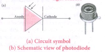
(ii) The direction of arrows indicates that the light is incident on the photo diode.
(iii) The device consists of a p-n junction semiconductor made of photosensitive material kept safely inside a plastic case as shown in fig.
(iv) It has a small transparent window that allows light to be incident on the p-n junction.
(v) Photodiodes car generate current when the p - n junction is exposed to light and hence are called as light sensors.
(vi) When a photon of sufficient energy (hv) strikes the depletion region of the diode, some of the valence band electron are elevated into conduction band, in turn holes are developed in the valence band. This creates electron-hole pairs. The amount of electron - hole pairs generated depends on the intensity of light incident on the p - n junction.
(vii) These electron and holes are swept across the p-n junction by the electric field created by reverse voltage before recombination takes place. Thus, holes move towards the n - side and electrons towards the P - side - when the external circuit is made, the electrons flow through the external circuit and constitute the photo current.
(viii) When the incident light is zero, there exists a reverse current which is negligible. This reverse current in the absence of any. incident light is called dark current and is. due to the thermally generated minority carriers.
21.
| Wireline | Wireless |
|---|---|
| Wireline communication (point-point communication) uses mediums like wires, cables, and optical fibers. | Wireless communication uses free space as a communication medium. |
| These systems cannot be used for long-distance transmission they are connected physically. | The signals are transmitted in the form of electromagnetic waves with the help of a transmitting antenna Hence wireless communication is used for long-distance transmission |
| Examples are telephone, intercom, and cable TV. | Examples are mobile, radio or TV broadcasting, and satellite communication. |
| Wireline up to 100 meters | Wireless up to several thousand kilometers |
It is the maximum distance between the source and the destination up to which the signal is received with sufficient strength.
22.
(i) Voltage regulators
(ii) Peak clippers
(iii) Calibrating voltages
23.
If the positive terminal battery is conneted to the n-side and the negative potential to the p-side, the junction is said to be reverse biased.
24.
Band of very large number of closely spaced energy levels in a very small energy range is known as energy band.
25.
\({ I }_{ B }=\frac { { V }_{ i } }{ { R }_{ B } } =\frac { 20V }{ 500k\Omega } =40\mu A\) [∵ VBE = 0V]
\({ I }_{ C }=\frac { { V }_{ CC } }{ { R }_{ C } } =\frac { 20V }{ 4k\Omega } =5mA\) [∵ VCE = 0V]
\(\beta =\frac { { I }_{ C } }{ { I }_{ B } } =\frac { 5mA }{ 40\mu A } =125\)
26.
\({ E }_{ g }=\frac { hc }{ \lambda } \)
Therefore,
\(\lambda =\frac { hc }{ { E }_{ g } } =\frac { 6.6\times { 10 }^{ -34 }\times 3\times { 10 }^{ 8 } }{ 1.875\times 1.6\times { 10 }^{ -19 } } \)
= 660 nm
The wavelength 660 nm corresponds to red colour light
27.
The P.D. between A and B is given by
\(V =\left[V_{\mathrm{A}}-V_{\mathrm{B}}\right]-V_{\mathrm{b}}(\mathrm{Si}) \)
\(=[3.3-(-7.4)]-0.7 \)
\(=10.7-0.7=10 \mathrm{~V} \)
The value of current flowing through AB can be obtained by using Ohm’s law
\(I=\frac { V }{ R } =\frac { 10}{ 1\times { 10 }^{ 3 } } ={ 10 }^{ -2 }A=10mA\)
28.
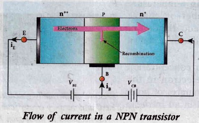
(i) The emitter-base junction is forward biased by a dc power supply Vm and the collector-based junction is reverse biased by the bias power supply VcB
(ii) The forward bias across the emitter base junction causes the majority charge carriers electrons in the emitter region to flow towards the base region and constitutes the emitter current (IE).
(iii) Since the base region is very narrow, most of the electrons reach the collector region.
(iv) The electrons that reach the collector region will be attracted by the collector terminal as it has positive potential and flows through the external circuit. This constitutes the collector current(Ic)
(v) The holes that are lost due to recombination in the base region ate replaced by the positive potential of the bias voltage VEE and constitute the base current (IB)
\( \mathrm{I}_{\mathrm{E}}=\mathrm{I}_{\mathrm{B}}+\mathrm{I}_{\mathrm{C}} \)
\(\mathrm{I}_{\mathrm{E}} \approx \mathrm{I}_{\mathrm{C}} \) \((\because \mathrm{I}_{\mathrm{B}} is\ very\ small )\)
29.
| S.No | Avalanche breakdown | Zener breakdown |
| (i) | Heavily doped p-n junctions have narrow depletion layers of the order of <10-6 m. | It occurs in lightly doped junctions Which have wide depletion layers. |
| (ii) | Electric field produced is strong in nature. | Weak electric field is produced. |
| (iii) | When a reverse voltage across the junction is increased to the breakdown limit, a very strong electric field is set up. It ruptures the covalent bonds in the lattice and thereby generating electronic-hole pairs. This effect is called Zener effect | Thermally generated minority charge carriers accelerated by the electric field gains sufficient kinetic energy, collide with the semiconductor atoms while passing through the depletion region. This leads to the breaking of covalent bonds and in turn covalent bonds and in turn generates electron-hole pairs |
| (iv) | Even a small further increases in reverse voltage produces a large number of charge carriers. Hence the junction has very low resistance in the breakdown region. | The newly generated charged carriers are also accelerated by the electric field resulting in more collisions and further production of charged carriers. |
| (v) | This process of emission of electrons due to the strong electric field is known as internal field emission or field ionization. | This cumulative process leads to an avalanche of charge carriers across the junction and consequently reduces the reverse resistance the diode current increases sharply. |
30.
The process of adding impurities to the instrinsic semiconductor is called doping.
31.
32.
RADAR stands for RAdio Detection And Ranging.
33.
(i) Radar basically stands for Radio Detection and Ranging System.
(ii) It is one of the important applications of communication systems' and is mainly used to sense, detect, and locate distant objects like aircraft, ships, spacecraft, etc.
(iii) The angle, range, or velocity of the objects that are invisible to the human eye can be determined.
(iii) Radar uses electromagnetic waves for communication. The electromagnetic signal is initially radiated into space by an antenna in all directions.
(iv) When this signal strikes the targeted object, it gets reflected or reradiated in many directions.
(v) This reflected (echo) signal is received by the radar antenna which in turn is delivered to the receiver.
(vi) Then, it is processed and amplified to determine the geographical statistics of the object. The range is determined by calculating the time taken by the signal to travel from RADAR to the target and back.
Applications :
Radars find extensive applications in almost all fields.
(i) In military, it is used for locating and detecting the targets.
(ii) It is used in navigation systems such as ship borne surface search, air search and weapons guidance systems.
(iii) To measure precipitation .rate and wind speed in meteorological observations, Radars are used.
(iv) It is employed to locate and rescue people in emergency situations.
34.
α = 0.98
ICu = 0.6 μA
\(\alpha =\frac { \beta }{ 1+\beta } \)
(or)
\(0.98=\frac { 1 }{ \frac { 1 }{ \beta } +1 } \)
β = 49
ICEO = (1 + β)ICBO
= (1 + 49) x 0.6μA
ICEO = 30 μA
= (1 + 49) x 0.6 μA
ICEO = 30 μA
IC = βIB+ ICEO
= 49 x 20 μA + 30 μA
IC = 1.01 mA
35.
Insulators:
(i) The valence band and the conduction band are separated by a large energy gap.
(ii) The forbidden energy gap is approximately 6 eV in insulators.
(iii) The gap is very large that electrons from valence band cannot move into conduction band even on the application of strong external electric field or the increase in temperature.
Metals
(i) In metals, the valence band and conduction band overlap.
(ii) Hence, electrons can move freely into the conduction band which results in a large number of free electrons in the conduction band.
Semiconductors
(i) In semiconductors, there exists a narrow forbidden energy gap (E < 3eV) between - g the valence band and the conduction band.
(ii) Free electrons are small in number, the conductivity of the semiconductors is not as high as that of the conductors.
36.
(i) This gives the variation of collector current (IC) with changes in base current (IB) at constant collector-emitter voltage (VCE).
(ii) It is seen that a small Ie flows even when IB is zero. This current is called the common emitter leakage current (ICEQ) which is due to the flow of minority charge carriers.
Forward current gain:
(i) The ratio of the change in collector current (ΔIC) to the change in base current (ΔIB) at constant collector-emitter voltage (VCE) is called forward current gain(β)
\(\beta ={ \left( \frac { \triangle { I }_{ C } }{ \triangle { I }_{ B } } \right) }_{ { V }_{ CE } }\)
(ii) It is value is very high and it generally ranges from 50 to 200. It depends on the construction of the transistors and will be provided by the manufacturer.
37.
Insulators
(i) The gap is very large that electrons from valence band cannot move into conduction band even on the application of strong external electric field or the increase in temperature.
(ii) The electrical conduction is not possible as the free electrons are almost nil.
(iii) Its resistivity is in the range of 1011 - 1019 Ωm
Metals
(i) Conduction becomes possible even at low temperatures.
(ii) The application of electric field provides sufficient energy to the electrons to drift in a particular' direction to constitute a current.
(iii) The resistivity value lies between 10-2 and 10-8Ωm
Semiconductors
(i) At a finite temperature, thermal agitations in the solid can break the covalent bond between the atoms.
(ii) This releases some electrons from valence band to conduction band
(iii) The resistivity value of semiconductors is from 10-5 to 10-6 Ωm
(iv) When the temperature is increased further, more number of electrons is promoted to the conduction band and increases the conduction.
(v) Thus, electrical conduction increases with the increase in temperature.
38.
(i) The transistor in saturation region acts as a closed switch while in cut-off region, it acts as an open switch.
(ii) It functions like an electronic switch that helps to turn ON or OFF a given circuit by a small control signal which keeps the transistor either in saturation region or in cut-off region.
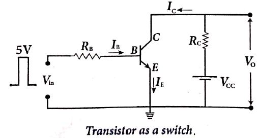
When the input is low:
(i) When the input is low (say 0 V), the base current is zero and transistor is not properly forward biased.
(ii) It is in cut off region, As a result, the collector current is zero and correspondingly the voltage drop across RC, also becomes nearly zero, The output voltage is high and Is equal to VCC.
(iii) It means that the no current flows through the transistor and it is said to be switched off. The transistor acts as an open switch.
When the input is high:
(i) When input voltage is increased to a certain high value (say +5 V), the base current (IB) increases and in turn decreases the collector current to its maximum.
(ii) The transistor will move into the saturation region. The increase in collector current (IC). increases the voltage drop across RC, thereby thereby lowering the output voltage, close to zero (since Vo = VCC -ICRC). It means that maximum current flows through the transistor and it is said to be switched on.
(iii)The transistor acts as a closed switch.
39.
HaIf wave rectifier:
Only one half of the input wave reaches the output. Therefore it is called half wave rectifier.
Construction:
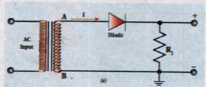
(i) The circuit consists of a transformer, a p-n junction diode and a resistor
(ii) In a half wave rectifier circuit, either a positive half or the negative half of the AC input is passed through by the diode while the other half is blocked
(iii) It acts as a rectifier diode.
.jpg)
(iv) Efficiency (η) is the ratio of the output DC power to the AC input power circuit. supplied to the circuit.
(v) The efficiency (η) of a half wave rectifier is found to be 40.6 %.
.jpg)
40.
i) AND gate
a) Circuit Symbol:
The circuit symbol of a two input AND gate is shown in Figure (a). A and B are inputs and Y is the output. It is a logic gate and hence A, B, and Y can have the value of either 1 or 0
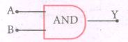
Two input AND gate
| Inputs | outputs | |
| A | B | Y = A + B |
| 0 | 0 | 0 |
| 0 | 1 | 0 |
| 1 | 0 | 0 |
| 1 | 1 | 1 |
Truth table
b) Boolean equation:
Y = A.B
It performs logical multiplication and is different from arithmetic multiplication.
c) Logic operation:
The output of AND gate is high only when all the inputs are high. In the rest of the cases, the output is low. It is represented in the truth table (Figure (b).
ii) OR gate
a) Circuit Symbol:
The circuit symbol of a two input OR gate is shown in Figure (a). A and B are inputs and Y is the output.
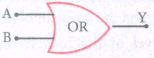
The input OR gate
| Inputs | outputs | |
| A | B | Y = A + B |
| 0 | 0 | 0 |
| 0 | 1 | 1 |
| 1 | 0 | 1 |
| 1 | 1 | 1 |
Truth table
a) Boolean equation:
A + B = Y
It performs logical addition and is different from arithmetic addition.
b) Logic operation:
The output of OR gate is high (logic 1 state) when either of the inputs or both are high. The truth table of OR gate is shown in Figure (a).
iii) NOT gate
a) Circuit Symbol:
The circuit symbol of NOT gate is shown in Figure (a). A and B are inputs and Y is the output.
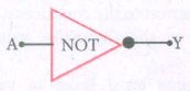
NOT gate
| Inputs | Output |
| A | Y = Ā |
| 0 | 1 |
| 1 | 0 |
Truth table
a) Boolean equation:
Y = Ā
b) Logic operation:
The output is the complement of the input. It is represented with an overbar. It is also called as inverter. The truth table infers that the output Y is I when input A is 0 and vice versa. The truth table of NOT is shown in Figure (b).
iv) NAND gate
a) Circuit Symbol:
The circuit symbol of NAND gate is shown in Figure (a). A and B are inputs and Y is the output.

Two input NAND gate
| Inputs | Output (AND) |
outputs (NAND) |
|
| A | B | Z = A.B | Y = \(\overline { A.B } \) |
| 0 | 0 | 0 | 1 |
| 0 | 1 | 0 | 1 |
| 1 | 0 | 0 | 1 |
| 1 | 1 | 1 | 0 |
Truth table
b) Boolean equation:
Y = \(\overline { A.B } \)
Logic operation:
The output Y equals, the complement of AND operation. The circuit is an AND gate followed by a NOT gate. Therefore, it is summarized as NAND. The output is at logic zero only when all the inputs are high. The rest of the cases, the output is high (Logic I state). The truth table of NAND gate is shown in Figure (b).
v) NOR gate
a) Circuit Symbol:
The circuit symbol of NOR gate is shown in Figure (a). A and B are inputs and Y is the output.

Two input NANS gate
| Inputs | Output (OR) |
outputs (NOR) |
|
| A | B | Z = A + B | Y = \(\overline { A+B } \) |
| 0 | 0 | 0 | 1 |
| 0 | 1 | 1 | 0 |
| 1 | 0 | 1 | 0 |
| 1 | 1 | 1 | 0 |
Truth table
Boolean equation:
Y = \(\overline { A+B } \)
Logic operation:
The output Y equals the complement of OR operation (A OR B). The circuit is an OR gate followed by a NOT gate and is summarized as NOR. The output is high when all the inputs are low. The output is low for all other combinations of inputs. The truth table of NOR gate is shown in Figure (b).
vi) Ex-OR gate
a) Circuit Symbol:
The circuit symbol of Ex-OR gate is shown in Figure (a). A and B are inputs and Y is the output. The Ex-OR operation is denoted as ⊕
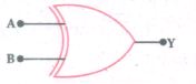
Ex-OR gate
| Inputs | outputs (Ex-OR) |
|
| A | B | Y = A ⊕ B |
| 0 | 0 | 0 |
| 0 | 1 | 1 |
| 1 | 0 | 1 |
| 1 | 1 | 0 |
Truth table
b) Boolean equation
Y = \(A.\overline { B } \) + \(\overline { A }.B \)
Y = A ⊕ B
Logic operation:
The output is high only when either of the two inputs is high. In the case of an Ex-OR gate with more than two inputs, the output will be high when odd number of inputs are high. The truth table of Ex-OR gate is shown in Figure (b).
41.
Fiber optic communication:
(i) The method of transmitting information from one place to another in terms of light pulses through an optical fiber is called fiber optic communication. It works on the principle of total internal reflection.
Applications:
(ii) Optical fiber system has a number of applications namely, international communication, inter-city communication, data links, plant and traffic control and defense applications.
(iii) Fiber cables are very thin and weigh lesser than copper cables.
(iv) This system has much larger band width. This means that its information carrying capacity is larger.
(v) Fiber optic system is immune to electrical interferences.
(vi) Fiber optic cables are cheaper than copper cables.
42.
(i) GPS stands for Global Positioning System. It is a global navigation satellite system that offers geolocation and time information to a GPS receiver anywhere on or near the Earth.
(ii) GPS system works the assistance of a satellite network.
(iii) Each of these satellites broadcasts a precise, signal and these signals convey the location data are received by a low-cost aerial which is then translated by the GPS software.
(iv) The software is able to recognize the satellite, its location, and the time taken by the signals to travel from each satellite.
(v) The software then processes the data it accepts from each satellite to estimate the location of the receiver.
Applications:
Global positioning system is highly useful in many fields such as fleet vehicle management (for tracking cars trucks and buses), wildlife management (for counting of wild animals), and engineering (for making tunnels, brides, etc).
43.
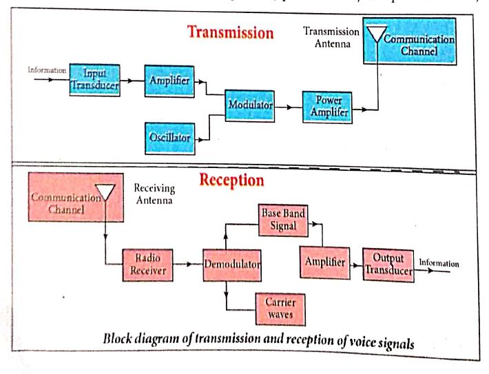
a) Information (Baseband or input signal):
i) Information can be in the form of a sound signal like speech, music, pictures, or computer data which is given as input to the input transducer.
b) Input transducer:
i) It converts the information which is in the form of sound, music, pictures or computer data into corresponding electrical signals.
ii) The electrical equivalent of the original information is called the baseband signal.
iii) The best example is the microphone that converts sound energy into electrical energy.
c) Transmitter
i) It feeds the electrical signal from the transducer to the communication channel
ii) It consists of circuits such as amplifier, oscillator, modulator, and power amplifier.
iii) Amplifier: The transducer output is very weak and is amplified by the amplifier.
iv) Oscillator: It generates high-frequency carrier wave (a sinusoidal wave) for long distance transmission into space. As the energy of a wave is proportional to its frequency, the carrier wave has very high energy.
v) Modulator: It superimposes the baseband signal onto the carrier signal and generates the modulated signal.
vi) Power amplifier: It increases the power level of the electrical signal in order to cover a large distance.
d) Transmitting antenna:
i) It radiates the radio signal into space in all directions.
ii) It travels in the form of electromagnetic waves with the speed of light.
e) Communication channel:
Communication channel is used to carry the electrical signal from transmitter to receiver with less noise or distortion.
Example: Wires, cables, optical fibres in wireline communication and free space in wireless communication.
f) Receiver:
i) The signals that are transmitted through the communication medium are received with the help of a receiving antenna and are fed into the receiver.
ii) The receiver consists of electronic circuits like demodulator, amplifier, detector etc. The demodulator extracts the baseband signal from the carrier signal.
iii) Then the baseband signal is detected and amplified using amplifiers.
iv) Finally, it is fed to the output transducer.
g) Repeaters:
i) Repeaters are used to increase the range or distance through which the signals are sent.
ii) It is a combination of transmitter and receiver.
iii) The signals are received, amplified, and retransmitted with a carrier signal of different frequency to the destination.
iv) The best example is the communication satellite in space
h) Output transducer:
i) It converts the electrical signal back to its original form such as sound, music, pictures or data.
ii) Examples of output transducers are loudspeakers, picture tubes, computer monitor, etc

12th Standard Syllabus & Materials
12th Standard
TN 12th Computer Applications களப்பெயர் முறைமை (DNS) Sample Question Papers Study Material - QB365 Set A
NEW12th Standard
TN 12th Computer Applications வலையமைப்பு எடுத்துக்காட்டுகள் மற்றும் நெறிமுறைகள் Sample Question Papers Study Material - QB365 Set A
NEW12th Standard
TN 12th Computer Applications கணினி வலையமைப்பு ஓர் அறிமுகம் Sample Question Papers Study Material - QB365 Set A
NEW12th Standard
TN 12th Computer Applications PHP-உடன் MySQL-ஐ இணைத்தல் Sample Question Papers Study Material - QB365 Set A



Tamilnadu Stateboard 12th Standard Subjects

Maths

Chemistry
Physics

Biology

Computer Science

Business Maths and Statistics

Economics

Commerce

Accountancy

History

Computer Applications
Biology
Computer Technology
Computer Applications
Computer Science
Business Maths and Statistics
Commerce
Economics
Maths
Chemistry
Physics
Computer Technology
History
Accountancy

Tamil

English

French
Tamilnadu Stateboard Standards

