
 100% FREE ACCESS
12th Standard Syllabus & Materials
12th Standard
TN 12th Computer Applications மின்னணு தரவு பரிமாற்றம் Sample Question Papers Study Material - QB365 Set A
NEW12th Standard
TN 12th Computer Applications மின் - வணிக பாதுகாப்பு அமைப்புகள் Sample Question Papers Study Material - QB365 Set A
NEW12th Standard
TN 12th Computer Applications மின்னணு செலுத்தல் முறைகள் Sample Question Papers Study Material - QB365 Set A
NEW12th Standard
TN 12th Computer Applications மின் - வணிகம் Sample Question Papers Study Material - QB365 Set A
NEW12th Standard
TN 12th Computer Applications திறந்த மூல கருத்துருக்கள் Sample Question Papers Study Material - QB365 Set A
NEW12th Standard
TN 12th Computer Applications வலையமைப்பு வடமிடல் Sample Question Papers Study Material - QB365 Set A

Published on: 26/01/2021
12th Standard Physics English Medium Reduced Syllabus Model Question paper - 2021 Part - 2
Download Tamil Nadu 12th Standard Physics question papers, model tests, one-mark questions, important questions, and public exam papers in PDF format. Free study materials and answer keys for TN State Board students.
Questions + Answers key
Take MCQ Physics Test1.
What is electronics?
2.
List out the laws of photo electric effect.
3.
State the laws of reflection
4.
Give and explain the mechanical analogy of LC oscillations by qualitative treatment.
5.
Obtain an expression for potential energy due to a collection of three point charges which are separated by finite distances.
6.
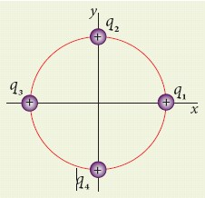
Consider four equal charges q1, q2, q3 and q4 = q = +1 μC located at four different points on a circle of radius 1m, as shown in the figure. Calculate the total force acting on the charge q1 due to all the other charges.
7.
ln NPN transistors, when the emitter-base junction is forward-biased, the direction of conventional current is from _____________
base to emitter
emitter to base
collector to base
base to collector
8.
Digital signals are converted into analog signals using ________.
FAX
Modem
Cable
Coaxial Cable
9.
In order to draw a transfer characteristics of transistors ________ is kept constant.
VCE
IB
IC
VBE
10.
Diffusion of free electrons across the junction of an unbiased diode produces _____________.
forward bias
reverse bias
depletion layer
break down
11.
In a p-n junction diode _________________.
the current in the reverse biased condition is generally very small
the current in the reverse biased condition is small but the forward biased current is independent of the biased voltage
the reverse biased current is strongly dependent on the applied bias voltage.
the forward biased current is very small in comparison to reverse biased current
12.
The cause of potential barrier in a p-n diode is ________________.
depletion of negative charges near the junction
concentration of positive charges near the junction
depletion of positive charges near the junction
concentration of positive and negative charges near the junction
13.
For a transistor amplifier, the voltage gain ______________.
remain constant for all frequencies
is high at high and low frequencies and constant in the mid - frequency range
is low at high and low frequencies and constant in the mid-frequency range
None of the above
14.
For Boolean identities match the pair
(i) \(\overset { = }{ A } \) (P) Ā + \(\bar { B } \)
(ii) \(\overline { A+B } \) (Q) A.B
(iii) \(\overline { A.B } \) (R) \(\bar { A } .\bar { B } \)
(iv) A.(Ā + B) (S) A
1 - (S), 2 (P), 3 - (Q), 4 - (R)
1 - (S), 2 (R), 3 - (Q), 4 - (P)
1 - (S), 2 (Q), 3 - (P), 4 - (R)
1- (S), 2 (R), 3 - (P), 4 - (Q)
15.
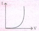
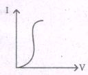
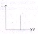
Which of the following figure represents an ideal diode characteristics?
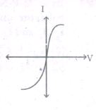
16.
In an N-P-N transistor circuit, the emitter, collector, and base current are respectively IE, IC, and lB. The relation between them is _____________.
IC
IB
IB > IC > IE
IB > IC > IE
17.
Digital circuits can be made to be respective use of ______________.
AND gate
OR gate
NOT gate
NAND gate
18.
A current gain for, a transistor working as CB amplifier is 0.90. If emitter current is 10 mA, then base current is ________________.
1mA
2 mA
0.1 mA
0.2 mA
19.
The electrical series circuit in digital form is
AND
OR
NOR
NAND
20.
In tuning radio we use,
capacitors
transistors
diodes
LEDS
21.
Two short bar magnets have magnetic moments 1.20 Am2 and 1.00 Am2 respectively. They are kept on a horizontal table parallel to each other with their north poles pointing towards south. They have a common magnetic equator and are separated by a distance of 20.0 cm. The value of the resultant horizontal magnetic induction at the mid-point O of the line joining their centres is (Horizontal components of Earth’s magnetic induction is 3.6 × 10⁻⁵ Wb m–2 )
3.60 × 10⁻⁵ Wb m-2
3.5 × 10⁻⁵ Wb m-2
2.56 × 10⁻⁴ Wb m-2
2.2 × 10⁻⁴ Wb m-2
22.
Prove the laws of reflection using Huygen's principle.
23.
For a BJT circuit shown, assume that the 'β' of the transistor is very large and VBE= 0.7 V. The mode of operation.
24.
Give circuit symbol, logical operation, truth table, and Boolean expression of
i) AND gate
ii) OR gate
iii) NOT gate
iv) NAND gate
v) NOR gate and
vi) EX-OR gate.
25.
Write the analogies between electrical and mechanical quantities
26.
Write thekey components of robot.
27.
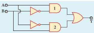
In the combination of the following gates, write the Boolean equation for output Y in terms of inputs A and B.
28.
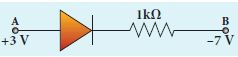
A silicon diode is connected with 1kΩ resistor as shown. Find the value of current flowing through AB is
29.
30.
Explain the need for a feedback circuit in a transistor oscillator.
31.
A diode is called as a unidirectional device. Explain.
1.
(i) It is the branch of physics incorporated with technology towards the design of circuits using transistors and microchips.
(ii) It depicts the behavior and movement of electrons in a semiconductor, vacuum, or gas.
(iii) Electronics deals with electrical circuits that involve active components such as transistors, diodes, integrated circuits, and sensors, associated with the passive components like resistors, inductors, capacitors, and transformers.
2.
(i) For a given frequency of incident light the number of photoelectrons emitted is directly proportional to the intensity of the incident light. The saturation current is also directly proportional to the intensity of incident light.
(ii) Maximum kinetic energy of the photo electrons is independent of intensity 0 the incident light.
(iii) Maximum kinetic energy of the photo electrons from a given metal is directly proportional to the frequency of incident light.
(iv) For a given surface, the emission of photoelectrons takes place only if the frequency of incident light is greater than a certain minimum frequency called the threshold frequency.
(v) There is no time lag between incidence of light and ejection of photo electrons.
3.
According to law of reflection,
(i) The incident ray, reflected ray and normal to the reflecting surface all are coplanar (ie. lie in the same plane).
(ii) The angle of incidence i is equal to the angle of reflection r.
i = r
4.
(i) The electromagnetic oscillations of LC system can be compared with the mechanical oscillations of a spring-mass system.
(ii) There are two forms of energy involved in LC oscillations. One is electrical energy of the charged capacitor; the other magnetic energy of the inductor carrying current.
(iii) Likewise, the mechanical energy of the spring-mass system exists in two forms; the potential energy of the compressed or extended spring and the kinetic energy of the mass. The Table lists these two pairs of energy.
(iv) By examining, the analogies between the various quantities can be understood and these correspondences.
(v) The angular frequency of oscillations of a spring-mass is given by equation
\(\omega =\sqrt { \frac { k }{ m } } \)
k ⟶ \(\frac { 1 }{ C } \) and m ⟶ L. Therefore, the angular frequency of LC oscillations is given by
ω = \(\frac { 1 }{ \sqrt { LC } } \)
5.
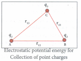
To calculate the total electrostatic potential energy, we use the following procedure. We bring all the charges one by one and arrange them according to the configuration as shown in Figure.
a) Bringing a charge q1 from infinity to the point A requires no work, because there are no other charges already present in the vicinity of charge q1.
b) To bring the second charge q2 to the point B, work must be done against the electric field created by the charge q1. So the work done on the charge q2 is W = q2 V1B. Here V1B is the electrostatic potential due to the charge q1 at point B.
\(U_I=\frac{1}{4\piε_o}\frac{q_1q_2}{r_{12}}\) .....(1)
Note that the expression is same when q2 is brought first and then q1 later.
c) Similarly to bring the charge q3 to the point C, work has to be done against the total electric field due to both the charges q1 and q2. So the work done to bring the charge q3 = q3 (V1C + V2C). Here V1C is the electrostatic potential due to charge q1 at point C and V2C is the electrostatic potential due to charge q2 at point C.
The electrostatic potential is
\(U_{II}=\frac{1}{4\piε_o}(\frac{q_1q_2}{r_{13}}+\frac{q_2q_3}{r_{23}})\) .....(2)
d) Adding equations (1) and (3), the total electrostatic potential energy for the system of three charges q1, q2 and q3 is
U = UI + UII
\(U=\frac{1}{4\piε_o}(\frac{q_1q_2}{r_{12}}+\frac{q_2q_3}{r_{13}}+\frac{q_2q_3}{r_{23}})\) ....(3)
6.
According to the superposition principle, the total electrostatic force on charge q1 is the vector sum of the forces due to the other charges,
\(\vec { { F }_{ 1 }^{ tot } } =\bar { { F }_{ 12 } } +\bar { { F }_{ 13 } } +\bar { F_{ 14 } } \)
The following diagram shows the direction of each force on the charge q1.
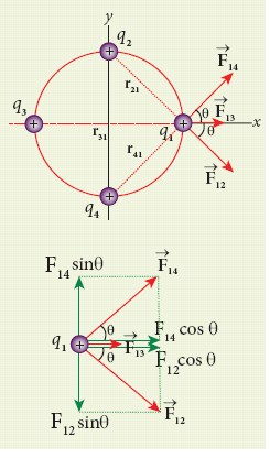
The charges q2 and q4 are equi-distant from q1. As a result the strengths (magnitude) of the forces \(\vec { { F }_{ 12 } } \) and \(\vec { { F }_{ 14 } } \) are the same even though their directions are different. Therefore the vectors representing these two forces are drawn with equal lengths. But the charge q3 is located farther compared to q2 and q4. Since the strength of the electrostatic force decreases as distance increases, the strength of the force \(\vec { { F }_{ 13 } } \) is lesser than that of forces \(\vec { { F }_{ 12 } } \) and \(\vec { { F }_{ 14 } } \). Hence the vector representing the force \(\vec { { F }_{ 13 } } \) is drawn with smaller length compared to that for forces \(\vec { { F }_{ 12 } } \) and \(\vec { { F }_{ 14 } } \).
From the figure, r21 =\(\sqrt { 2 } \) m = r41 and r31 = 2m
The magnitudes of the forces are given by
F13 = \(\frac { kq^{ 2 } }{ r_{ 31 }^{ 2 } } =\frac { 9\times 10^{ 9 }\times 10^{ -12 } }{ 4 } \)
F13 = 2.25 x 10⁻³ N
F12 = \(\frac { kq^{ 2 } }{ r_{ 31 }^{ 2 } } ={ F }_{ 14 }=\frac { 9\times 10^{ 9 }\times 10^{ -12 } }{ 2 } \)
= 4.5 x 10⁻³N
From the figure, the angle θ = 450. In terms of the components, we have
\(\vec { { F }_{ 12 } } ={ F }_{ 12 }cos\theta \hat { i } -{ F }_{ 12 }sin\theta \hat { j } \)
= 4.5 x 10⁻³ x \(\frac { 1 }{ \sqrt { 2 } } \hat { i-4.5\times { 10 }^{ -3 }\times \frac { 1 }{ \sqrt { 2 } } \hat { j } } \)
\(\vec { { F }_{ 13 } } =F_{ 13 }\hat { i } \) = 2.25 x 10⁻³ N\(\hat { i } \)
\(\vec { { F }_{ 14 } } ={ F }_{ 14 }cos\theta \hat { i } +{ F }_{ 14 }sin\theta \hat { j } \)
= 4.5 x 10⁻³ x \(\frac { 1 }{ \sqrt { 2 } } \hat { i+4.5\times { 10 }^{ -3 }\times \frac { 1 }{ \sqrt { 2 } } \hat { j } } \)
Then the total force on q1 is,
\(\vec { { F }_{ 1 }^{ tot } }={ (F }_{ 12 }cos\theta \hat { i } -{ F }_{ 12 }sin\theta \hat { j } )+{ F }_{ 13 }\hat { i } +{ (F }_{ 14 }cos\theta \hat { i } +{ F }_{ 14 }sin\theta \hat { j } )\)
\(\vec { { F }_{ 1 }^{ tot } } =({ F }_{ 12 }cos\theta +F_{13}+{ F }_{ 14 }cos\theta )\hat { i } +(-{ F }_{ 12 }sin\theta +{ F }_{ 14 }sin\theta )\)\(\hat { j } \)
Since F12 = F14, the j th component is zero.
Hence we have
\(\vec { { F }_{ 1 }^{ tot } } =({ F }_{ 12 }cos\theta +F_{13}+{ F }_{ 14 }cos\theta )\hat { i } \)
substituting the values in the above equation,
\(\left( \frac { 4.5 }{ \sqrt { 2 } } +2.25+\frac { 4.5 }{ \sqrt { 2 } } \right) \times10^{-3}\hat { i }=(4.5\sqrt { 2 } +2.25)\times 10^{-3}\hat { i } \)
\(\vec { { F }_{ 1 }^{ tot } } \) = 8.61 x 10⁻³ N\(\hat { i } \)
The resultant force is along the positive x-axis.
7.
(a)
base to emitter
8.
(b)
Modem
9.
(a)
VCE
10.
(c)
depletion layer
11.
(c)
the reverse biased current is strongly dependent on the applied bias voltage.
12.
(d)
concentration of positive and negative charges near the junction
13.
Directions : Question numbers 53, 54, 55 are based on following passage.
PASSAGE : ANPN transistor is used in common emitter made in an amplifier circuit. A change of 40 HA in the base current changes the output current by 2 mA and 0.04 V in input voltage.
14.
(d)
1- (S), 2 (R), 3 - (P), 4 - (Q)
15.
(a)
16.
(b)
IB
17.
(d)
NAND gate
18.
\(\begin{array}{l} \alpha=\frac{I_c}{I_{\mathrm{c}}} ; \mathrm{I}_{\mathrm{c}}=\alpha \mathrm{I}_{\mathrm{t}}=9 \mathrm{~mA} \\ \mathrm{I}_{\mathrm{B}}=\mathrm{I}_{\mathrm{t}}-\mathrm{I}_{\mathrm{c}}=10-9=1 \mathrm{~mA} \end{array}\)
19.
(a)
AND
20.
(a)
capacitors
21.
(c)
2.56 × 10⁻⁴ Wb m-2
22.
(i) Consider a parallel beam of light, incident on a reflecting plane surface such as a plane mirror XY as shown in Figure.
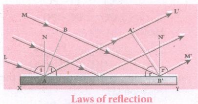
(ii) The incident wavefront is AB and the reflected wavefront is A'B' in the same medium. These wavefronts are perpendicular to the incident rays L, M and reflected rays L', M' respectively.
(iii) By the time point A of the incident wavefront touches the reflecting surface, point B is yet to travel a distance BB' to touch the reflecting surface a B'.
(iv) When point B falls on the reflecting surface at H', point A would have reached A.
(v) This is applicable to all the points on the wavefront. Thus, the reflected wavefront A'B' emanates as a plane wavefront. The two normals Nand N' are considered at the points where the rays Land Mfallon the reflecting surface.
(vi) As reflection happens in the same medium, the speed of light is the same before and after the reflection.
(vii) Hence, the time is taken for the ray to travel from B to B' is the same as the time taken for the ray to travel from A to A'.
(viii) Thus, the distance BB' is equal to the distance AA'; (A~A' = BB').
(a) The incident rays, the reflected rays, and the normal are in the same plane.
(b) Angle of incidence,\(\angle i=\angle NAL={ 90 }^{ o }-\angle NAB=\angle BAB'\)
Angle of reflection,
∠r= ∠N' B' M' = 900 - ∠N' B' A' = A' B' A'
(ix) For the two right-angle triangles, ΔABB' and ΔB' A' A', the right angles, ∠B and ∠A' are equal, (∠B and∠A = 900); the two sides, ∠A' and ∠B' are equal, (AA'= BB'); the side AB' is common.
(x) Thus, the two triangles are congruent. As per the property of congruency, the two angles, ∠BAB' and A' B' A' must also be equal.
i = r
Hence, the laws of reflection are proved.
23.
VBE =0.7V
Input junction is a forward biased.
Since,
VBE = 0.7V
VCE = VBE+ VCB
VCB = VCE-VBE
To determine VCB we find IC
\({ I }_{ C }\cong { I }_{ C }\frac { 2-{ V }_{ BE } }{ { R }_{ 2 } } =\frac { 2-0.7 }{ 1k\Omega } \)
IC = 1.3mA
VCE = VCC - IC (R1 + R2)
= 10 - 1.3mA (10K + 1K)
VCE = - 4.3 V
VCE =-4.3V-0.7
VCB = - 5V
24.
i) AND gate
a) Circuit Symbol:
The circuit symbol of a two input AND gate is shown in Figure (a). A and B are inputs and Y is the output. It is a logic gate and hence A, B, and Y can have the value of either 1 or 0
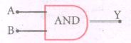
Two input AND gate
| Inputs | outputs | |
| A | B | Y = A + B |
| 0 | 0 | 0 |
| 0 | 1 | 0 |
| 1 | 0 | 0 |
| 1 | 1 | 1 |
Truth table
b) Boolean equation:
Y = A.B
It performs logical multiplication and is different from arithmetic multiplication.
c) Logic operation:
The output of AND gate is high only when all the inputs are high. In the rest of the cases, the output is low. It is represented in the truth table (Figure (b).
ii) OR gate
a) Circuit Symbol:
The circuit symbol of a two input OR gate is shown in Figure (a). A and B are inputs and Y is the output.
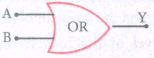
The input OR gate
| Inputs | outputs | |
| A | B | Y = A + B |
| 0 | 0 | 0 |
| 0 | 1 | 1 |
| 1 | 0 | 1 |
| 1 | 1 | 1 |
Truth table
a) Boolean equation:
A + B = Y
It performs logical addition and is different from arithmetic addition.
b) Logic operation:
The output of OR gate is high (logic 1 state) when either of the inputs or both are high. The truth table of OR gate is shown in Figure (a).
iii) NOT gate
a) Circuit Symbol:
The circuit symbol of NOT gate is shown in Figure (a). A and B are inputs and Y is the output.
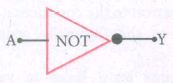
NOT gate
| Inputs | Output |
| A | Y = Ā |
| 0 | 1 |
| 1 | 0 |
Truth table
a) Boolean equation:
Y = Ā
b) Logic operation:
The output is the complement of the input. It is represented with an overbar. It is also called as inverter. The truth table infers that the output Y is I when input A is 0 and vice versa. The truth table of NOT is shown in Figure (b).
iv) NAND gate
a) Circuit Symbol:
The circuit symbol of NAND gate is shown in Figure (a). A and B are inputs and Y is the output.

Two input NAND gate
| Inputs | Output (AND) |
outputs (NAND) |
|
| A | B | Z = A.B | Y = \(\overline { A.B } \) |
| 0 | 0 | 0 | 1 |
| 0 | 1 | 0 | 1 |
| 1 | 0 | 0 | 1 |
| 1 | 1 | 1 | 0 |
Truth table
b) Boolean equation:
Y = \(\overline { A.B } \)
Logic operation:
The output Y equals, the complement of AND operation. The circuit is an AND gate followed by a NOT gate. Therefore, it is summarized as NAND. The output is at logic zero only when all the inputs are high. The rest of the cases, the output is high (Logic I state). The truth table of NAND gate is shown in Figure (b).
v) NOR gate
a) Circuit Symbol:
The circuit symbol of NOR gate is shown in Figure (a). A and B are inputs and Y is the output.

Two input NANS gate
| Inputs | Output (OR) |
outputs (NOR) |
|
| A | B | Z = A + B | Y = \(\overline { A+B } \) |
| 0 | 0 | 0 | 1 |
| 0 | 1 | 1 | 0 |
| 1 | 0 | 1 | 0 |
| 1 | 1 | 1 | 0 |
Truth table
Boolean equation:
Y = \(\overline { A+B } \)
Logic operation:
The output Y equals the complement of OR operation (A OR B). The circuit is an OR gate followed by a NOT gate and is summarized as NOR. The output is high when all the inputs are low. The output is low for all other combinations of inputs. The truth table of NOR gate is shown in Figure (b).
vi) Ex-OR gate
a) Circuit Symbol:
The circuit symbol of Ex-OR gate is shown in Figure (a). A and B are inputs and Y is the output. The Ex-OR operation is denoted as ⊕
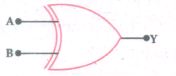
Ex-OR gate
| Inputs | outputs (Ex-OR) |
|
| A | B | Y = A ⊕ B |
| 0 | 0 | 0 |
| 0 | 1 | 1 |
| 1 | 0 | 1 |
| 1 | 1 | 0 |
Truth table
b) Boolean equation
Y = \(A.\overline { B } \) + \(\overline { A }.B \)
Y = A ⊕ B
Logic operation:
The output is high only when either of the two inputs is high. In the case of an Ex-OR gate with more than two inputs, the output will be high when odd number of inputs are high. The truth table of Ex-OR gate is shown in Figure (b).
25.
|
Electrical system |
Mechanical system |
|---|---|
| Charge q | Displacement x |
| Current i = \(\frac { dq }{ dt } \) | Velocity v = \(\frac { dx }{ dt } \) |
| Inductance L | Mass m |
| Reciprocal of capacitance \(\frac { 1 }{ C } \) | Force constant k |
| Electrical energy = \(\frac { 1 }{ 2 } \left( \frac { 1 }{ C } \right) { q }^{ 2 }\) | Potential energy = \(\frac { 1 }{ 2 } k{ x }^{ 2 }\) |
| Magnetic energy = \(\frac { 1 }{ 2 } \) Li2 | Kinetic energy = \(\frac { 1 }{ 2 } \) mv2 |
| Electromagnetic energy = \(U=\frac { 1 }{ 2 } \left( \frac { 1 }{ C } \right) { q }^{ 2 }\) + \(\frac12\)Li2 | Mechanic energy E = \(\frac { 1 }{ 2 } k{ x }^{ 2 }\) + \(\frac { 1 }{ 2 } \) mv2 |
26.
The key components of a robot are Power conversion unit, Actuators, Electric motors, Pneumatic Air Muscles, Muscle wires, Piezo Motors and Ultrasonic Motors, Sensors, and Robot locomotion.
27.
The output at the 1st AND gate : A\(\overline { B } \)
The output at the 2nd AND gate : ĀB
The output at the OR gate: Y = A. \(\overline { B } \) + Ā .B
28.
The P.D. between A and B is given by
\(V =\left[V_{\mathrm{A}}-V_{\mathrm{B}}\right]-V_{\mathrm{b}}(\mathrm{Si}) \)
\(=[3.3-(-7.4)]-0.7 \)
\(=10.7-0.7=10 \mathrm{~V} \)
The value of current flowing through AB can be obtained by using Ohm’s law
\(I=\frac { V }{ R } =\frac { 10}{ 1\times { 10 }^{ 3 } } ={ 10 }^{ -2 }A=10mA\)
29.
30.
(i) If the portion of the output fed to the input is in phase with the input, then the magnitude of the input signal increases
(ii) It is necessary for sustained oscillations.
31.
When a PN junction diode is forward biased, the depletion region decreases and the diode conduct once after the barrier potential is crossed, when it is reverse biased the depletion region increases and the diode does not conduct sci it is called as unidirectional device.

12th Standard Syllabus & Materials
12th Standard
TN 12th Computer Applications களப்பெயர் முறைமை (DNS) Sample Question Papers Study Material - QB365 Set A
NEW12th Standard
TN 12th Computer Applications வலையமைப்பு எடுத்துக்காட்டுகள் மற்றும் நெறிமுறைகள் Sample Question Papers Study Material - QB365 Set A
NEW12th Standard
TN 12th Computer Applications கணினி வலையமைப்பு ஓர் அறிமுகம் Sample Question Papers Study Material - QB365 Set A
NEW12th Standard
TN 12th Computer Applications PHP-உடன் MySQL-ஐ இணைத்தல் Sample Question Papers Study Material - QB365 Set A



Tamilnadu Stateboard 12th Standard Subjects

Maths

Chemistry
Physics

Biology

Computer Science

Business Maths and Statistics

Economics

Commerce

Accountancy

History

Computer Applications
Biology
Computer Technology
Computer Applications
Computer Science
Business Maths and Statistics
Commerce
Economics
Maths
Chemistry
Physics
Computer Technology
History
Accountancy

Tamil

English

French
Tamilnadu Stateboard Standards

