
 100% FREE ACCESS
12th Standard Syllabus & Materials
12th Standard
TN 12th Maths Applications of Matrices and Determinants Sample Question Papers Study Material - QB365 Set A
NEW12th Standard
TN 12th Computer Applications மின்னணு தரவு பரிமாற்றம் Sample Question Papers Study Material - QB365 Set A
NEW12th Standard
TN 12th Computer Applications மின் - வணிக பாதுகாப்பு அமைப்புகள் Sample Question Papers Study Material - QB365 Set A
NEW12th Standard
TN 12th Computer Applications மின்னணு செலுத்தல் முறைகள் Sample Question Papers Study Material - QB365 Set A
NEW12th Standard
TN 12th Computer Applications மின் - வணிகம் Sample Question Papers Study Material - QB365 Set A
NEW12th Standard
TN 12th Computer Applications திறந்த மூல கருத்துருக்கள் Sample Question Papers Study Material - QB365 Set A

Published on: 28/11/2025
Download Tamil Nadu 12th Standard Physics question papers, model tests, one-mark questions, important questions, and public exam papers in PDF format. Free study materials and answer keys for TN State Board students.
Questions + Answers key
Take MCQ Physics Test
1.
How many photons per second emanate from a 50 mW laser of 640 nm?
2.
3.
Determine the wavelength of light emitted from LED which is made up of GaAsP semiconductor whose forbidden energy gap is 1.875 eV. Mention the colour of the light emitted (Take h = 6.6 x 10⁻³⁴ Js).
4.
A straight metal wire crosses a magnetic field of flux 4 mWb in a time 0.4 s. Find the magnitude of the emf induced in the wire.
5.
Compute the magnitude of the magnetic field of a long, straight wire carrying a current of 1 A at distance of 1m from it. Compare it with Earth’s magnetic field.
6.
Two materials X and Y are magnetised whose values of intensity of magnetisation are 500 A m–1 and 2000 A m–1 respectively. If the magnetising field is 1000 A m–1, then which one among these materials can be easily magnetized?
7.
A potential difference across 24 Ω resistor is 12 V. What is the current through the resistor?
8.
Derive the expression for the force between two parallel, current - carrying conductors.
9.
State and prove De Morgan’s first and second theorem.
10.
Give circuit symbol, logical operation, truth table, and Boolean expression of
i) AND gate
ii) OR gate
iii) NOT gate
iv) NAND gate
v) NOR gate and
vi) EX-OR gate.
11.
Discuss about the simple microscope and obtain the equations for magnification for near point focusing and normal focusing.
12.
Derive an expression for electrostatic potential due to an electric dipole.
13.
Obtain the condition for bridge balance in Wheatstone’s bridge.
14.
Consider a point charge +q placed at the origin and another point charge -2q placed at a distance of 9 m from the charge +q. Determine the point between the two charges at which electric potential is zero.
15.
An e.m. wave is propagating in a medium with a velocity \(\vec{v}=v \hat{i}\). The instantaneous oscillating electric field of this e.m. wave is along + y-axis, then the direction of oscillating magnetic field of the e.m. wave will be along _____.
–y direction
–x direction
+z direction
–z direction
16.
The potential energy of magnetic dipole whose dipole moment is \(\vec{p}_{m}=(-0.5 \hat{i}+0.4 \hat{j}) \mathrm{Am}^{2}\) kept in uniform magnetic field \(\vec{B}=0.2 \hat{i} \mathrm{~T}\).
–0.1 J
–0.8 J
0.1 J
0.8 J
17.
The unit of focal power of a lens is ______________.
Watt
Horse Power
Dioptre
Lux
18.
If charge of 60 C passes through a bulb for 4 minutes then the current flows through it is ____________.
1 A
0.5 A
0.25 A
0.75 A
19.
The direction of dipole moment vector is
from zero to infinity
from infinity to zero
from negative charge to positive charge
from positive charge to negative charge
20.
Skip distance the shortest distance between ______________.
the point of transmission and the point of reception
the uplink and the downlink station
the transmitter and the target
the receiver and the target
21.
The moderator used in nuclear reactor is ________________.
Cadmium
Boron oxide
Heavy water
Uranium
22.
The energy of the electron in the first orbit of hydrogen atom is -13.6 eV. Its potential energy is _______________.
-13.6 eV
13.6eV
-27.2 eV
27.2 eV
23.
The half-life period of a radioactive element A is same as the mean life time of another radioactive element B. Initially both have the same number of atoms. Then _____.
A and B have the same decay rate initially
A and B decay at the same rate always
B will decay at faster rate than A
A will decay at faster rate than B
24.
The ratio between the radius of first three orbits of hydrogen atom is _____.
1:2:3
2:4:6
1:4:9
1:3:5
25.
A light source of wavelength 520 nm emits 1.04 x 10¹⁵ photons per second while the second source of 460 nm produces 1.38 x 10¹⁵ photons per second. Then the ratio of power of second source to that of first source is _____.
1.00
1.02
1.5
0.98
26.
27.
An object is placed in front of a convex mirror of focal length off and the maximum and minimum distance of an object from the mirror such that the image formed is real and magnified.
2f and c
c and \(\infty\)
f and O
None of these
28.
\(\frac{20}{\pi^2}H\) inductor is connected to a capacitor of capacitance C. The value of C in order to impart maximum power at 50 Hz is
50 μF
0.5 μF
500 μF
5 μF
29.
When the current changes from +2A to −2A in 0.05 s, an emf of 8 V is induced in a coil. The co-efficient of self-induction of the coil is
0.2H
0.4H
0.8H
0.1H
30.
A parallel plate capacitor stores a charge Q at a voltage V. Suppose the area of the parallel plate capacitor and the distance between the plates are each doubled then which is the quantity that will change?
Capacitance
Charge
Voltage
Energy density
1.
P = 50 mW; λ = 640nm = 640 x 10-9 m
P = 50 x 10-3W
\(n=\cfrac { hc }{ \lambda } = \frac{6.626 \times10^{-34} \times 3 \times 10^8}{640 \times 10{-9}}=3.106 \times 10^{-19}J\)
\(n=\frac{E}{hv}=\cfrac { 50\times { 10 }^{ -3 } }{ 3.106\times { 10 }^{ -19 } } = 1.61\times 10^{17} s^{-1}\)
n = 1.61 x 10¹⁷ s-I
2.
3.
\({ E }_{ g }=\frac { hc }{ \lambda } \)
Therefore,
\(\lambda =\frac { hc }{ { E }_{ g } } =\frac { 6.6\times { 10 }^{ -34 }\times 3\times { 10 }^{ 8 } }{ 1.875\times 1.6\times { 10 }^{ -19 } } \)
= 660 nm
The wavelength 660 nm corresponds to red colour light
4.
Change in magnetic flux, dф = 4 x 10⁻³ Wb
Change in time, dt = 0.4 s
Magnitude of Induced emf \(= |\frac { -d\Phi }{ dt }|=\frac { d\Phi }{ dt }\)
\(=\frac { 4\times 10^{ -3 } }{ 0.4 } \) = 10 x 10-3 V = 10 mv
∴ Magnitude of induced emf =10 mV
5.
Given that I = 1 A and radius r = 1 m
Bstraightwire = \(=\frac { { \mu }_{ ° }I }{ 2\pi r } =\frac { 4\pi \times { 10 }^{ -7 }\times 1 }{ 2\pi \times 1 } =2\times { 10 }^{ -7 }T\)
But the Earth’s magnetic field is Bearth \(\sim { 10 }^{ -5 }T\)
So, Bstraightwire is one hundred times smaller than BEarth.
6.
The susceptibility of material X is
Xm,x = \(\frac { \left| \overset { \rightarrow }{ M } \right| }{ \left| \overset { \rightarrow }{ H } \right| } =\frac { 500 }{ 1000 } =0.5\)
The susceptibility of material Y is
Xm,y = \(\frac { \left| \overset { \rightarrow }{ M } \right| }{ \left| \overset { \rightarrow }{ H } \right| } =\frac { 2000 }{ 1000 } =2\)
Since, susceptibility of material Y is greater than that of material X, material Y can be easily magnetized than X.
7.
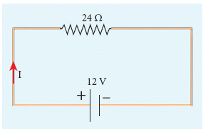
V = 12 V and R = 24 Ω
Current, I = ?
From Ohm’s law, \(I=\frac{V}{R}=\frac{12}{24}=0.5A\)
8.
Two long straight parallel current-carrying conductors separated by a distance r are kept in air medium. Let I1 and I2 be the electric currents passing through the conductors A and B is same direction (i.e., along z-direction) respectively. The net magnetic field at a distance r due to current I1 in conductor A is
\(\vec{B}_{1}=\frac{\mu_{o} I_{1}}{2 \pi r}(-\hat{\mathrm{i}})=-\frac{\mu_{o} I_{1}}{2 \pi r} \hat{i}\)
.JPG)
From thumb rule, the direction of magnetic field is perpendicular to the plane of the paper and inwards (arrow into the page ⊗) i.e. along negative \(\vec{i}\)direction
Let us consider a small elemental length dl in conductor B at which the magnetic field \(\vec{B}_1\) present, From equation \(\overrightarrow{d F}=(I \overrightarrow{d l} \times \vec{B})\)
Lorentz force on the element dl of conductor B is
\(\overrightarrow{d F}=\left(I_{2} d \vec{l} \times \vec{B}_{1}\right)=-I_{2} d l \frac{\mu_{o} I_{1}}{2 \pi r}(\hat{k} \times \hat{i})=-\frac{\mu_{o} I_{1} I_{2} d l}{2 \pi r} \hat{j}\)
Therefore the force on dl of wire conductor B is directed towards the conductor A. So the element of length dl in B is attracted towards the conductor A. Hence, the force per unit length of the conductor B due to the current in the conductor A is,
\(\frac{\vec{F}}{l}=-\frac{\mu_{o} I_{1} I_{2}}{2 \pi r} \hat{j}\)
Similarly, the net magnetic induction due to current I2 (in conductor B) at a distance r in the elemental length dl of conductor A is
\(\vec{B}_{2}=\frac{\mu_{o} I_{2}}{2 \pi r} \hat{i}\)
From the thumb rule direction of magnetic field is perpendicular to the plane of the paper and outwards (arrow out to the page ⊙) i.e., along positive \(\vec{i}\)direction.
Hence the magnetic force at element dl of the conductor A is,
\(\vec{dF} =\left(I_{1} \vec{d} l \times \vec{B}_{2}\right)=I_{1} d l \frac{\mu_{o} I_{2}}{2 \pi r}(\hat{k} \times \hat{i}) \)
\(=\frac{\mu_{o} I_{1} I_{2} d l}{2 \pi r} \hat{j} \)
Therefore the force on dl of conductor A is directed towards the conductor B. So the length dl is attracted towards the conductor B as shown in Figure.
.JPG)
The force acting per unit length of the conductor A due to the conductor B is
\(\frac{\vec{F}}{l}=-\frac{\mu_{0} I_{1} I_{2}}{2 \pi r} \hat{j}\)
Attractive force: The direction of electric current is same.
Repulsive force: The direction of electric current is opposite.
9.
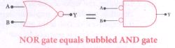
First Theorem :
The complement of the sum of two logical inputs is equal to the product of its complements.
\(\overline { A+B } \) = \(\bar { A } .\bar { B } \)
Proof:
(i) The Boolean equation for NOR gate is Y = \(\overline { A+B } \)
(ii) The Boolean equation for a bubbled AND gate is Y =\(\bar { A } .\bar { B } \)
(iii) Both cases generate same outputs for same inputs. It can be verified using the following truth
| A | B | A+B | \(\overline { A+B } \) | Ā | \(\bar { B } \) | \(\bar { A } .\bar { B } \) |
| 0 | 0 | 0 | 1 | 1 | 1 | 1 |
| 0 | 1 | 1 | 0 | 1 | 0 | 0 |
| 1 | 0 | 1 | 0 | 1 | 0 | 0 |
| 1 | 1 | 1 | 0 | 0 | 0 | 0 |
(i) From the above truth table, we can conclude \(\overline { A+B } \) = \(\bar { A } .\bar { B } \)
(ii) Thus De Morgan's first theorem is proved.
(iii) Hence, a NOR gate is equal to a bubbled AND gate
Second theorem :
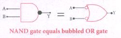
The complement of the product of two is equal to the sum of its complements
\(\overline { A.B } \) = \(\bar { A } +\bar { B } \)
Proof:
(i) The Boolean equation for NAND gate is Y = \(\overline { A.B } \)
(ii) The Boolean equation for bubbled OR gate is Y = \(\bar { A } +\bar { B } \)
(iii) A and B are the inputs and Y is the output. The above two equations produces the same output for the same inputs. It can be verified by using the truth table.
| A | B | A+B | \(\overline{\mathrm{A}. \mathrm{B}}\) | Ā | \(\bar { B } \) | \(\overline{\mathrm{A}}+\overline{\mathrm{B}}\) |
| 0 | 0 | 0 | 1 | 1 | 1 | 1 |
| 0 | 1 | 0 | 1 | 1 | 0 | 1 |
| 1 | 0 | 0 | 1 | 0 | 1 | 1 |
| 1 | 1 | 1 | 0 | 0 | 0 | 0 |
(i) From the above truth table, we can conclude \(\overline { A.B } \) = \(\bar { A } +\bar { B } \)
(ii) Thus, De Morgan's second therom is proved.
(iii) Hence, a NAND gate is equal to a bubbled OR gate.
10.
i) AND gate
a) Circuit Symbol:
The circuit symbol of a two input AND gate is shown in Figure (a). A and B are inputs and Y is the output. It is a logic gate and hence A, B, and Y can have the value of either 1 or 0
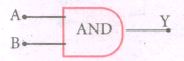
Two input AND gate
| Inputs | outputs | |
| A | B | Y = A + B |
| 0 | 0 | 0 |
| 0 | 1 | 0 |
| 1 | 0 | 0 |
| 1 | 1 | 1 |
Truth table
b) Boolean equation:
Y = A.B
It performs logical multiplication and is different from arithmetic multiplication.
c) Logic operation:
The output of AND gate is high only when all the inputs are high. In the rest of the cases, the output is low. It is represented in the truth table (Figure (b).
ii) OR gate
a) Circuit Symbol:
The circuit symbol of a two input OR gate is shown in Figure (a). A and B are inputs and Y is the output.
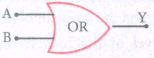
The input OR gate
| Inputs | outputs | |
| A | B | Y = A + B |
| 0 | 0 | 0 |
| 0 | 1 | 1 |
| 1 | 0 | 1 |
| 1 | 1 | 1 |
Truth table
a) Boolean equation:
A + B = Y
It performs logical addition and is different from arithmetic addition.
b) Logic operation:
The output of OR gate is high (logic 1 state) when either of the inputs or both are high. The truth table of OR gate is shown in Figure (a).
iii) NOT gate
a) Circuit Symbol:
The circuit symbol of NOT gate is shown in Figure (a). A and B are inputs and Y is the output.
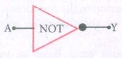
NOT gate
| Inputs | Output |
| A | Y = Ā |
| 0 | 1 |
| 1 | 0 |
Truth table
a) Boolean equation:
Y = Ā
b) Logic operation:
The output is the complement of the input. It is represented with an overbar. It is also called as inverter. The truth table infers that the output Y is I when input A is 0 and vice versa. The truth table of NOT is shown in Figure (b).
iv) NAND gate
a) Circuit Symbol:
The circuit symbol of NAND gate is shown in Figure (a). A and B are inputs and Y is the output.

Two input NAND gate
| Inputs | Output (AND) |
outputs (NAND) |
|
| A | B | Z = A.B | Y = \(\overline { A.B } \) |
| 0 | 0 | 0 | 1 |
| 0 | 1 | 0 | 1 |
| 1 | 0 | 0 | 1 |
| 1 | 1 | 1 | 0 |
Truth table
b) Boolean equation:
Y = \(\overline { A.B } \)
Logic operation:
The output Y equals, the complement of AND operation. The circuit is an AND gate followed by a NOT gate. Therefore, it is summarized as NAND. The output is at logic zero only when all the inputs are high. The rest of the cases, the output is high (Logic I state). The truth table of NAND gate is shown in Figure (b).
v) NOR gate
a) Circuit Symbol:
The circuit symbol of NOR gate is shown in Figure (a). A and B are inputs and Y is the output.

Two input NANS gate
| Inputs | Output (OR) |
outputs (NOR) |
|
| A | B | Z = A + B | Y = \(\overline { A+B } \) |
| 0 | 0 | 0 | 1 |
| 0 | 1 | 1 | 0 |
| 1 | 0 | 1 | 0 |
| 1 | 1 | 1 | 0 |
Truth table
Boolean equation:
Y = \(\overline { A+B } \)
Logic operation:
The output Y equals the complement of OR operation (A OR B). The circuit is an OR gate followed by a NOT gate and is summarized as NOR. The output is high when all the inputs are low. The output is low for all other combinations of inputs. The truth table of NOR gate is shown in Figure (b).
vi) Ex-OR gate
a) Circuit Symbol:
The circuit symbol of Ex-OR gate is shown in Figure (a). A and B are inputs and Y is the output. The Ex-OR operation is denoted as ⊕
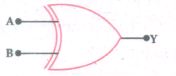
Ex-OR gate
| Inputs | outputs (Ex-OR) |
|
| A | B | Y = A ⊕ B |
| 0 | 0 | 0 |
| 0 | 1 | 1 |
| 1 | 0 | 1 |
| 1 | 1 | 0 |
Truth table
b) Boolean equation
Y = \(A.\overline { B } \) + \(\overline { A }.B \)
Y = A ⊕ B
Logic operation:
The output is high only when either of the two inputs is high. In the case of an Ex-OR gate with more than two inputs, the output will be high when odd number of inputs are high. The truth table of Ex-OR gate is shown in Figure (b).
11.
(i) A simple microscope is a single magnifying (converging) lens of small focal length. To get an erect, magnified and virtual image of the object.
(ii) For this the object is placed between the focal length Fand P on one side of the lens and viewed from other side of the lens. There are two magnifications to be discussed for two kinds of focusing.
(a) Near point focusing:
The eye is least strained when image is formed at near point,i.e. 25 cm. The near point is also called as least distance of distinct vision. This is shown in Figure.
.JPG)
Magnification in near point focusing:
(i) Object distance u is less than f
(ii) The image distance is the near point D. The magnification m is given by the relation,
\(m=\cfrac { v }{ u } \) ...............(1)
Substituting, V = - D and u= - u, as both the distances are measured to the left of the lens. Hence,
\(m=\cfrac { -D }{ -u }\)
\(m=\cfrac { D }{ u } \) ...............(2)
Using lens equation, W.K.T, m = 1 - (v/f)
Substiuting v = -D gives, \(\\ m=1+\cfrac { D }{ f } \) ..................(3)
This is the magnification for near point focusing.
(b) Normal focusing :
(i) The eye is most relaxed when the image is formed at infinity. The focusing is called normal focusing when the image is formed at infinity. This is shown in Figure (b).
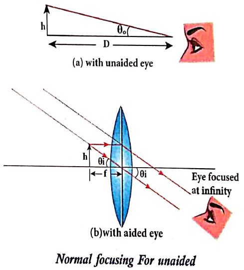
Magnification in normal focusing (angular magnification):
(ii) The angular magnification is defined as the ratio of angle θ1 subtended by the image with aided eye to the angle θ0 subtended by the object with unaided eye.
\(m=\cfrac { { \theta }_{ 1 } }{ { \theta }_{ 0 } } \) .........(2)
For unaided eye shown in Figure (a),
\(tan\theta _{ 0 }\approx { \theta }_{ 1 }=\cfrac { h }{ D } \) ................(3)
For aided eye shown in Figure(b).
\(tan\theta _{ i }={ \theta }_{ i }=\cfrac { h }{ f } \) ...................(4)
The angular magnification is,
\(m=\cfrac { { \theta }_{ i } }{ { \theta }_{ o } } =\cfrac { h/f }{ h/D } \)
\(m=\cfrac { D }{ f } \) ..............(5)
This is the magnification for normal focusing.
12.
Electrostatic potential at a point due to an electric dipole :
(i) Consider two equal and opposite charges separated by a small distance 2a as shown in Figure. The point P is located at a distance r from the midpoint 'O' of the dipole. Let θ be the angle between the line OP and dipole axis AB.

(ii) Let r1 be the distance of point P from +q and r2 be the distance of point P from -q.
Potential at P due to charge +q\(=\frac { 1 }{ 4\pi { \varepsilon }_{ 0 } } \frac { q }{ { r }_{ 1 } } \)
Potential at P due to charge -q \(=-\frac { 1 }{ 4\pi { \varepsilon }_{ 0 } } \frac { q }{ { r }_{ 2 } } \)
Total potential at the point P,
\(V=\frac { 1 }{ 4\pi { \varepsilon }_{ 0 } } q\left( \frac { 1 }{ { r }_{ 1 } } -\frac { 1 }{ { r }_{ 2 } } \right) \) ....(1)
(iii) Suppose if the point P is far away from the dipole, such that (r >> a), then equation (1) can be expressed in terms of r.
By the cosine law for triangle BOP,
\({ r }_{ 1 }^{ 2 }={ r }^{ 2 }+{ a }^{ 2 }-2ra cos\theta \)
\({ r }_{ 1 }^{ 2 }={ r }^{ 2 }\left( 1+\frac { { a }^{ 2 } }{ { r }^{ 2 } } -\frac { 2a }{ r } cos\theta \right) \)
Since the point P is very far from dipole, then(r >> a). Then term \(\frac{a^{2}}{r^{2}}\)
\({ r }_{ 1 }^{ 2 }={ r }^{ 2 }\left( 1-2a\frac { cos\theta }{ r } \right) \)
\((or){ r }_{ 1 }=r{ \left( 1-\frac { 2a }{ r } cos\theta \right) }^{ \frac { 1 }{ 2 } }\)
\(\frac { 1 }{ { r }_{ 1 } } =\frac { 1 }{ r } { \left( 1-\frac { 2a }{ r } cos\theta \right) }^{ -\frac { 1 }{ 2 } }\)
iv) Since \(\frac{a}{r}\) << 1, we can use binomial theorem and retain the terms up to first order.
\(\frac { 1 }{ { r }_{ 1 } } =\frac { 1 }{ r } \left( 1+\frac { a }{ r } cos\theta \right) ...(2)\)
Similarly applying the cosine law for triangle AOP,
r22 = r2 + a2 - 2ra cos (180-θ)
Since cos(180 - θ) = - cos θ we get
r22= r2 + a2 + 2ra cos θ
Neglecting the term \(\frac { { a }^{ 2 } }{ { r }^{ 2 } } \) because (r >> a)
\({ r }_{ 2 }^{ 2 }={ r }^{ 2 }\left( 1+\frac { 2acos\theta }{ r } \right) \)
\({ r }_{ 2 }=r{ \left( 1+\frac { 2acos\theta }{ r } \right) }^{ \frac { 1 }{ 2 } }\)
Using Binomial theorem, we get
\(\frac { 1 }{ { r }_{ 2 } } =\frac { 1 }{ r } \left( 1-a\frac { cos\theta }{ r } \right) \quad \quad ...(3)\)
Substituting equation (3) and (2) in equation (1),
\(V=\frac { 1 }{ 4\pi { \varepsilon }_{ 0 } } q\left( \frac { 1 }{ r } \left( 1+a\frac { cos\theta }{ r } \right) -\frac { 1 }{ r } \left( 1-a\frac { cos\theta }{ r } \right) \right) \)
\(V=\frac { q }{ 4\pi { \varepsilon }_{ 0 } } \left( \frac { 1 }{ r } \left( 1+a\frac { cos\theta }{ r } -1+a\frac { cos\theta }{ r } \right) \right) \)
\(V=\frac { 1 }{ 4\pi { \varepsilon }_{ 0 } } \frac { 2aq }{ { r }^{ 2 } } cos\theta \)
v)
\(V=\frac { 1 }{ 4\pi { \varepsilon }_{ 0 } } \left( \frac { pcos\theta }{ { r }^{ 2 } } \right) \)
Now we can write p cos\(\theta =\vec { p } .\hat { r } \) where \(\hat { r } \) is the unit vector from the point O to point P. Hence the electric potential at a point P due to an electric dipole is given by
\(V=\frac { 1 }{ 4\pi { \varepsilon }_{ 0 } } \frac { \vec { p } .\hat { r } }{ { r }^{ 2 } } (r>>a)\quad ...(4)\)
Equation (4) is valid for distances very large compared to the size of the dipole. But for a point dipole, the equation (4) is valid for any distance.
Special cases:
Case (i) : If the point P lies on the axial line of the dipole on the side of +q, then θ = 0. Then the electric potential becomes
\(V=\frac { 1 }{ 4\pi { \varepsilon }_{ 0 } } \frac { p }{ { r }^{ 2 } } \quad \quad ...(5)\)
Case (ii) : If the point P lies on the axial line of the dipole on the side of -q, then θ = 180°, then
\(V=-\frac { 1 }{ 4\pi { \varepsilon }_{ 0 } } \frac { p }{ { r }^{ 2 } } \quad \quad ...(6)\)
Case (iii) : If the point P lies on the equatorial line of the dipole, then θ = 90°. Hence,
V = 0 .....(7)
13.
Wheatstone's bridge:
i) An important application of Kirchhoff's rule is Wheatstone's bridge. It is used to compare Resistances and also helps in determining the unknown resistance in electrical network. The bridge consists of four resistances P, Q, R and S connected as shown in Figure.
ii) A galvanometer G is connected between the points B and D. The battery is connected between the points A and C. The current through the galvanometer is IG and its resistance is G.
Applying Kirchhoff's current rule to junction B
I1 - IG - I3 = 0 ..(1)
Applying Kirchhoff's current rule to junction D,
I2 + IG - I4 = 0 ...(2)
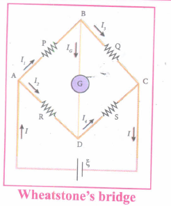
Applying Kirchhoff's voltage rule to loop ABDA,
I1P + IGG - I2R = 0 ...(3)
Applying Kirchhoff's voltage rule to loop ABCDA,
I1P + I3Q - I4S - I2R = 0 ...(4)
(iii) When the points B and D are at the same potential, the bridge is said to be balanced. As there is no potential difference between B and D, no current flows through galvanometer (IG = 0). Substituting IG = 0 in equation (1), (2) and (3), we get
I1 = I3 ..(5)
I2 = I4 ..(6)
I1P = I2R ..(7)
Substituting the equation (7) in equation (4),
I3Q = I4S .....(8)
Dividing equation (7) by equation (8), we get
\(\cfrac { P }{ Q } =\cfrac { R }{ S } \) .....(9)
(iv) This is the bridge balance condition. Only under this condition, galvanometer shows null deflection.
14.
According to the superposition principle, the total electric potential at a point is equal to the sum of the potentials due to each charge at that point.
Consider the point at which the total potential zero is located at a distance x from the charge +q as shown in the figure.
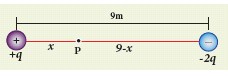
The total electric potential at P is zero.
Vtot = \(\frac { 1 }{ 4\pi { \varepsilon }_{ 0 } } \left( \frac { q }{ x } -\frac { 2q }{ (9-x) } \right) \)=0
Which gives \(\frac { q }{ x } -\frac { 2q }{ (9-x) } \)
or \(\frac { 1 }{ x } =\frac { 2 }{ (9-x) } \)
Hence, x = 3m
15.
(c)
+z direction
16.
U =\(\vec{p_m}.\vec {B}\)
U = -(0.5\(\hat{i}\) + 0.4\(\hat{j}\)).(0.2\(\hat{j}\))
U = 0.1 J
17.
(c)
Dioptre
18.
\(I=\frac{Q}{t}=\frac{60}{4 \times 60}=0.25 \mathrm{~A}\)
19.
(c)
from negative charge to positive charge
20.
(a)
the point of transmission and the point of reception
21.
(c)
Heavy water
22.
\(U_0=2 E_s=2(-13.6 \mathrm{eV})=-27.2 \mathrm{eV}\)
23.
TA1/2 = ፒB
\(\frac{0.6931}{\lambda_{\mathrm{A}}}=\frac{1}{\lambda_{\mathrm{B}}} \)
\(\lambda_{\mathrm{B}}=\frac{\lambda_{\mathrm{A}}}{0.6931}=1.44 \lambda_{\mathrm{A}}\)
Hence, B will decay at faster rate than A
24.
rn ∞ n2
r1: r2: r3 = 1: 4: 9
25.
\(P =\frac{E}{t}=\frac{n h v}{t}=\frac{n h c}{\lambda t} \Rightarrow P \propto n / t \)
\(\frac{P_1}{P_2} =\frac{1.38 \times 10^{15}}{460} \times \frac{520}{1.04 \times 10^{15}}=1.5\)
26.
(b)
27.
Convex Mirror is diverging in nature and for all positions of objects, convex mirror forms virtual and erect image.
28.
\(L=\frac{20}{\pi^2} \mathrm{H}, \mathrm{f}=50 \mathrm{~Hz} \)
\(f=\frac{1}{2 \pi \sqrt{L C}} \)
\(50=\frac{1}{2 \pi \sqrt{\frac{20}{\pi^2} \times C}} \)
\(50=\frac{1}{2 \times \sqrt{20 C}} \)
\(\therefore(50)^2=\frac{1}{4 \times 20 C} \)
\(\therefore C=\frac{1}{2500 \times 4 \times 20}=5 \times 10^{-6}=5 \mu \mathrm{F}\)
29.
\(\text {emf } e=8 \mathrm{~V} \)
\(d I=I_1-I_0=2-(-2)=4 \mathrm{~A} \)
\(\text {dt }=0.05 \mathrm{~s} \)
\(L=\frac{-e}{d I / d t}=\frac{-8}{4 / 0.05} \)
\(=\frac{-8 \times 0.05}{4}=\frac{-0.40}{4} \)
=-0.1 H
-ve sign indicates that self-induced emf always opposes the current w.r.t. time.
30.
Energy density uE \(=\frac{U}{volume}\)
If A' = 2A d ' = 2d
Then V ' = 2A x 2d = 4Ad = 4V
Then volume would be increased. So, energy density will change.

12th Standard Syllabus & Materials
12th Standard
TN 12th Computer Applications வலையமைப்பு வடமிடல் Sample Question Papers Study Material - QB365 Set A
NEW12th Standard
TN 12th Computer Applications களப்பெயர் முறைமை (DNS) Sample Question Papers Study Material - QB365 Set A
NEW12th Standard
TN 12th Computer Applications வலையமைப்பு எடுத்துக்காட்டுகள் மற்றும் நெறிமுறைகள் Sample Question Papers Study Material - QB365 Set A
NEW12th Standard
TN 12th Computer Applications கணினி வலையமைப்பு ஓர் அறிமுகம் Sample Question Papers Study Material - QB365 Set A



Tamilnadu Stateboard 12th Standard Subjects

Maths

Chemistry
Physics

Biology

Computer Science

Business Maths and Statistics

Economics

Commerce

Accountancy

History

Computer Applications
Biology
Computer Technology
Computer Applications
Computer Science
Business Maths and Statistics
Commerce
Economics
Maths
Chemistry
Physics
Computer Technology
History
Accountancy

Tamil

English

French
Tamilnadu Stateboard Standards


