100% FREE ACCESS
12th Standard CBSE Syllabus & Materials
12th Standard CBSE
CBSE 12th Economics Government Budget and the Economy Previous year Question Papers Study Material - QB365 Set A
NEW12th Standard CBSE
CBSE 12th Computer Science Interface Python with MySQL - New Previous year Question Papers Study Material - QB365 Set A
NEW12th Standard CBSE
CBSE 12th Computer Science Database Concept - New Previous year Question Papers Study Material - QB365 Set A
NEW12th Standard CBSE
CBSE 12th Computer Science Data Communication - New Previous year Question Papers Study Material - QB365 Set A
NEW12th Standard CBSE
CBSE 12th Computer Science Data Structures - New Previous year Question Papers Study Material - QB365 Set A
NEW12th Standard CBSE
CBSE 12th Computer Science Functions - New Previous year Question Papers Study Material - QB365 Set A

Published on: 12/08/2019
Electronic Devices
Download CBSE Class 12th Standard CBSE Physics question papers, sample papers, important questions, and previous year solved papers in PDF format. Get free study materials, NCERT solutions, and exam preparation resources for Class 12th Standard CBSE Physics
Questions + Answers key
Take MCQ Physics Test
1.
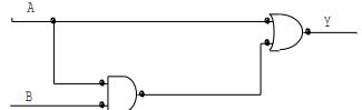
Express by a truth table the output Y for all possible inputs A and B in the circuit shown below
2.
The ratio of number of free electrons to holes ne/nh for two different materials A and B are 1 and <1 respectively. Name the type of semi conductor to which A and B belongs.
3.
In transistor a current controlled (or)temperature controlled device?.
4.
Which semiconductor has more mobility : \(p\)-type or \(n\)-type? Explain.
5.
How does the energy gap of an intrinsic semiconductor vary, when doped with a pentavalent impurity?
6.
Is Ohm's law obeyed in semiconductor or not?
7.
According to energy band diagram, what makes a substance
(a) conductor
(b) insulator?
8.
The transistor is operated in common emitter configuration at \(\mu A\) to 200 \(\mu A\) produces a change in the collector current from 5 mA to 10 mA. The current gain is
100
150
50
75
9.
The electrical conductivity of a semiconductor increases when electromagnetic radiation of wavelength shorter than 2480 nm is incident on it. The band gap (in e V) for the semiconductor is
0.9
0.7
0.5
1.1
10.
A p-type semiconductor is obtained by doping silicon with
germanium
gallium
bismuth
Phosphorus
11.
In an n-type semiconductor, the Fermi level lies 0.3 e V below the conduction band at 300 k. If the temperature is increased to 330 k, where does the new position of the Fermi level lie?
0.55 e V below the conduction band
0.44 eV below the conduction band
0.33 eV below the conduction band
0.27 eV below the conduction band
12.
The conduction band in a solid is partially filled at 0 k. The solid sample is
Conductor
Semiconductor
Insulator
none of these
13.
A pure semiconductor germanium or silicon,free of every impurity is called intrinsic semiconductor, At room temperature, a pure semiconductor has a very small number of current carriers (electrons and holes).Hence,its conductivity is low.
When the impurity atoms of valence five or three are doped in a pure semiconductor,we get respectively \(n-\) type or \(p-\) type extrinsic semiconductor.In case of a doped semiconductor.\({ n }_{ e }n_{ h }={ n }_{ i }^{ 2 };\)when \({ n }_{ e }\) and \(n_{ h }\) are the number density of electrons and holes respectively and \({ n }_{ i }\) is the number density of intrinsic charge carriers in a pure semiconductor. The conductivity of extrinsic semiconductor is much higher than that that of intrinsic semiconductor.
Read the above passage and answer the following question:
(i) Name two materials to be doped in pure semiconductor of silicon to get (a) \(p-\)type semiconductor (b) \(n-\)type semiconductor
(ii) What do you learn from the above study?
14.
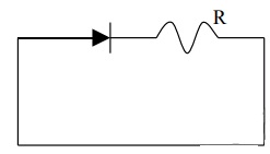
The diode shown in the figure has a constant voltage drop of 0.5V at all currents and a maximum power rating of 100mW. What should be the value of resistance R connected in series, for maximum current.?
1.
The output of the AND gate is Y = A.B consequently the input of the OR gate are A and A.B . Then the final Y = A + A.B
| A | B | Y =A.B | A | Y | Y = A +Y |
|---|---|---|---|---|---|
| 0 | 0 | 0 | 0 | 0 | 0 |
| 0 | 1 | 0 | 0 | 0 | 0 |
| 1 | 0 | 0 | 1 | 0 | 1 |
| 1 | 1 | 1 | 1 | 1 | |
2.
If ne/nh = 1. Hence A is intrinsic semi conductor.
If ne/nh < 1, ne < nh hence B is P-type
3.
Transistor is a current controlled devices
4.
The mobility of electrons in \(n\)-type semiconductor is more than the mobility of holes in \(p\)-type semiconductor. Since the \(n\)-type semiconductor has electrons as majority carriers and holes as minority carriers, whereas the \(p\)-type semiconductor has holes as majority carriers and electrons as minority carriers, therefore mobility of \(n\)-type is more than that of \(p\)-type.
5.
When an intrinsic semiconductor is doped with the impurity atoms of valence five like As, P or Sb, some additional energy levels are produced, situated in the energy gap slightly below the conduction band which are called donor energy levels. Due to it, energy gap in semiconductor decreases.
6.
In semiconductors, Ohms law is obeyed only for low electric field (less than \(10^{ 6 }Vm-1) \). Above this field, the current becomes almost independent of applied field, hence Ohm's law is not obeyed in semiconductors.
7.
(a) Overlapping of conduction band and valence band
(b) A large energy gap (more than 3 eV) Between conduction band and valence band.
8.
(b)
150
9.
(c)
0.5
10.
(b)
gallium
11.
(d)
0.27 eV below the conduction band
12.
Conductor
13.
(i) (a) The doping of pure silicon with boron or aluminium will give us \(p-\)type semiconductor
(b) The doping of pure silicon with arsenic or phosphorous will give us \(n-\)type semiconductor.
(ii) From the above study, we find that to get better output current ,pure semiconductor has to be adopted with suitable (impurity) atoms.Similarly,in day to day life,the appearence of right kind of persons(leaders) in society can improve their lot.
14.
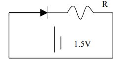
e.m.f of the source , E = 1.5
Voltage drop across the diode , Vd = 0.5 V
Maximum power rating of the diode
I = (P / Vd)
I = 0.2A
Potential drop across resistance R
V = E - Vd
= 1 V
R = V/1 = 1/0.2 = 5 \(\Omega \)

12th Standard CBSE Syllabus & Materials
12th Standard CBSE
CBSE 12th Computer Science Python Revision Tour I - New Previous year Question Papers Study Material - QB365 Set A
NEW12th Standard CBSE
CBSE 12th Business Studies Planning Important Questions And Answers Study Material - QB365 Set A
NEW12th Standard CBSE
CBSE 12th Business Studies Business Environment Important Questions And Answers Study Material - QB365 Set A
NEW12th Standard CBSE
CBSE 12th Business Studies Principles of Management Important Questions And Answers Study Material - QB365 Set A



CBSE 12th Standard CBSE Subjects
CBSE Standards