100% FREE ACCESS
12th Standard CBSE Syllabus & Materials
12th Standard CBSE
CBSE 12th Economics Government Budget and the Economy Previous year Question Papers Study Material - QB365 Set A
NEW12th Standard CBSE
CBSE 12th Computer Science Interface Python with MySQL - New Previous year Question Papers Study Material - QB365 Set A
NEW12th Standard CBSE
CBSE 12th Computer Science Database Concept - New Previous year Question Papers Study Material - QB365 Set A
NEW12th Standard CBSE
CBSE 12th Computer Science Data Communication - New Previous year Question Papers Study Material - QB365 Set A
NEW12th Standard CBSE
CBSE 12th Computer Science Data Structures - New Previous year Question Papers Study Material - QB365 Set A
NEW12th Standard CBSE
CBSE 12th Computer Science Functions - New Previous year Question Papers Study Material - QB365 Set A

Published on: 25/10/2025
Download CBSE Class 12th Standard CBSE Physics question papers, sample papers, important questions, and previous year solved papers in PDF format. Get free study materials, NCERT solutions, and exam preparation resources for Class 12th Standard CBSE Physics
Questions + Answers key
Take MCQ Physics Test
1.
C,Si and Ge have same lattice structure. Why is C insulator while Si and Ge intrinsic semiconductor?
2.
Why is the semiconductor damaged by a strong current?
3.
Can we take one slab of p-type semiconductor and physically join it to another n-type semiconductor to get p-n junction?
4.
Suppose a pure Si crystal has \(5\times 10^{ 28 }\) atmos \(m^{ -3 }\). It is doped by ppm concentration of pentavalent As. Calculate the number of electrons and holes. Given that \({ n }_{ i }=1.5\times { 10 }^{ 16 }m^{ 3 }\)
5.
When a forward bias applied to a p-n junction, it
(a) raises the potential barrier
(b) reduces the majority carrier current to zero
(c) lowers the potential barrier
(d) None of the above
6.
If a p-n junction diode is reverse biased.
the potential barrier is lowered
the potential barrier rermainsunaffected.
the potential barrier is raised
the current is mainly due to majority charge carriers.
7.
The formation of depletion region in a p-n junction diode is due to
movement of dopant atoms
diffusion of the electrons and holes
drift of electrons only
drift of holes only
8.
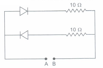
A 2V battery is connected across the points A and B as shown in the figure. Assuming that the resistance of each diode is zero in forward bias and infinity in reverse bias, the current supplied by the battery when its positive terminal is connected to A is
0.2 A
0.4 A
Zero
0.1 A
9.
The forbidden energy band gap in conductors, semiconductors and insulators are EG1, EG2 and EG3 respectively. The relation among them is
EG1 = EG2 = EG3
EG1 < EG2 < EG3
EG1 > EG2 > EG3
EG1 < EG2 > EG3
10.
The potential barrier of germanium diode is
0.1 V ,
0.3 V
0.5 V
0.7 V
11.
A npn transistor is connected in common emitter configuration in a give amplifier. A load resistance of \(800\Omega \) is connected in the collector circuit and the voltage drop across is 0.8 V. If the current amplification factor is 0.96 and the input resistance of the circuit is \(192 \ \Omega \), the voltage gain and the power gain of the amplifier will respectively be
4,3.84
3.69, 3.84
4, 4
4,3.69
12.
c and si both have same lattice structure,having 4 bonding electrons in each Howeever, c is insulator where as si is intrinsic semiconductor. This is because:
In case of \(c\) the valence band is not completely filled at absolute zero temperature
In case of \(c\) the conduction band is partly filled even at absolute zero temperature
The four bonding electrons in the case of \(c\) lie in the second orbit,whereas in the c case of \(si\) they lie in the third orbit.
The four bonding electrons in the case of \(c\) lie in the third orbit,whereas for \(si\) they lie in the fourth orbit.
13.
The built in potential of p-n junction diode is a function of
temperature
biased voltage
doping density
all of the above
14.
Which type of semiconductor is obtained by mixing arsenic with silicon?
\(n-type\)
\(p-type\)
Both
None
15.
Carbon, silicon and germanium have four valence electrons each. These are characterised by valence and conduction bands separated by energy band gap respectively equal to (Eg) C, (Eg) Si and (Eg) Ge. Which of the following statements is true?
\(\text { (a) }\left(E_{g}\right)_{\mathrm{Si}}<\left(E_{g}\right)_{\mathrm{Ge}}<\left(E_{g}\right)_{\mathrm{C}}\)
\(\text { (b) }\left(E_{g}\right)_{\mathrm{C}}<\left(E_{g}\right)_{\mathrm{Ge}}>\left(E_{g}\right)_{\mathrm{Si}}\)
\(\text { (c) }\left(E_{g}\right)_{\mathrm{C}}>\left(E_{g}\right)_{\mathrm{Si}}>\left(E_{g}\right)_{\mathrm{Ge}}\)
\(\text { (d) }\left(E_{g}\right)_{\mathrm{C}}=\left(E_{g}\right)_{\mathrm{Si}}=\left(E_{g}\right)_{\mathrm{Ge}}\)
16.
Which of the statements given In an n-type silicon, which of the following statement is true for p-type semiconductos.
(a) Electrons are majority carriers and trivalent atoms are the dopants.
(b) Electrons are minority carriers and pentavalent atoms are the dopants.
(c) Holes are minority carriers and pentavalent atoms are the dopants.
(d) Holes are majority carriers and trivalent atoms are the dopants.
17.
In half wave rectification , what is the output frequency if the input frequency is 50 Hz. What is the output frequency of a full wave rectification for the same input frequency.
18.
(i) How is a photodiode fabricated?
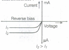
(ii) Briefly explain its working. Draw its V-I characteristics for two different intensities of illumination.
19.
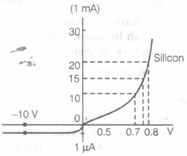
The V-I characteristic of a silicon diode is as shown in the figure. Calculate the resistance of the diode at
(i) I = 15 mA and
(ii) V = -10 V
20.
The current gain of a transistor in a common base arrangement is 0.95, find the voltage gain and power gain if the load resistance of output circuit is 400 k\(K\Omega \) and the input rsistance is 200 \(\Omega \) .
21.
From the output characteristics shown in Fig.(b), calculate the values of \(\beta\)ac and \(\beta\)dc of the transistor when VCE is 10 V and I C = 4.0 mA
22.
Draw a circuit diagram of an n- p-n transistor with its emitter base junction forward biased and base- collector junction reverse biased. Describe briefly its working. Explain, how a transistor in active state exhibits a low resistance at its emitter-base junction and high resistance at its base-collector junction?
23.
Sanjay was preparing an electronic project for science exhibition. He required to light the LED using a 6 V supply. LEDs need only a very small current to make them light and they do not heat up in use. So he put a resistor in series to limit the current. Then there would be p.d. of 4 V across the resistor as there is always 2.0 V across the LED itself when it is conducting. The current should be 10 mA through both LED and the resistor. He could use the resistance by equation, R = V/I to calculate the value of R.
\(R=\frac { V }{ I } =\frac { 4V }{ 10mA } =\frac { 4V }{ 0.01A } =400V\)
Thus the protecting resistor should be around 400 \(\Omega \)
(a) What are the values exhibited by Sanjay?
(b) A semiconductor has equal electron and hole concentration of \(6\times 10^{ 8 }/m^{ 3 }\) . On doping with certain impurity, electron concentration increases to \(9\times 10^{ 12 }/m^{ 3 }\) .
(i) Identify the new semiconductor obtained after doping.
(ii) Calculate the new hole concentration.
(iii) How does the energy gap vary with doping?
24.
The potential barrier in the p-n junction diode is the barrier in which the charge recquires additional force for crossing the region. In other words, the barrier in which the charge carrier stopped by the obstructive force is known as the potential barrier.
When a p-type semiconductor is brought into a close contact with n-type semiconductor, we get a p-n junction with a barrier potential 0.4 V and width of depletion region is 4.0 x 10⁻⁷ m. This p-n junction is forward biased with a battery of voltage 3V and negligible internal resistance, in series with a resistor of resistance R, ideal millimeter and key K as shown in figure. When key is pressed, a current of 20 mA passes through the diode.
(i) The intersity of the electric field in the depletion region when p-n junction is unbiased is
| (a) 0.5 x 10⁶ V m-1 | (b) 1.0 x 10⁶ V m-1 | (c) 2.0 x 10⁶ V m-1 | (d) 1.5 x 10⁶ V m-1 |
(ii) The resistance of resistor R is
| (a) 150 \(\Omega\) | (b) 300 \(\Omega\) | (c) l30 \(\Omega\) | (d) 180 \(\Omega\) |
(iii) In a p-n junction, the potential barrier is due to the charges on either side of the junction, these charges are
| (a) majority carriers | (b) minority carriers |
| (c) both (a) and (b) | (d) fixed donor and acceptor ions. |
(iv) If the voltage of the potential barrier is V0 A voltage V is applied to the input, at what moment will the barrier disappear?
| (a) V |
(b) V=V0 | (c) V>V0 | (d) V< |
(v) If an electron with speed 4.0 x 10⁵ m s-1 approaches the p-n junction from the n-side, the speed with which it will enter the p-side is
| (a) 1.39 x 10⁵ m S-1 | (b) 2.78 x 10⁵ m S-1 | (c) 1.39 x 10⁶ m S-1 | (d) 2.78 x 10⁶ m s-1 |
25.
From Bohr's atomic model, we know that the electrons have well defined energy levels in an isolated atom. But due to interatomic interactions in a crystal, the electrons of the outer shells are forced to have energies different from those in isolated atoms. Each energy level splits into a number of energy levels forming a continuous band.The gap between top of valence band and bottom of the conduction band in which no allowed energy levels for electrons can exist is called energy gap.
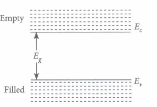
(i) In an insulator energy band gap is
| (a) Eg = 0 | (b) Eg< 3eV | (c) Eg > 3eV | (d) None of the above |
(ii) In a semiconductor, separation between conduction and valence band is of the order of
| (a) 0 eV | (b) 1 eV | (c) 10 eV | (d) 50 eV |
(iii) Based on the band theory of conductors, insulators and semiconductors, the forbidden gap is smallest in
| (a) conductors | (b) insulators | (c) semiconductors | (d) All of these |
(iv) Carbon, silicon and germanium have four valence electrons each. At room temperature which one of the following statements is most appropriate?
| (a) The number of free electrons for conduction is significant only in Si and Ge but small in C. |
| (b) The number of free conduction electrons is significant in C but small in Si and Ge. |
| (c) The number of free conduction electrons is negligibly small in all the three. |
| (d) The number offree electrons for conduction is significant in all the three. |
(v) Solids having highest energy level partially filled with electrons are
| (a) semiconductor | (b) conductor | (c) insulator | (d) none of these |
1.
The 4 bonding electrons of C, Si or Ge lie, respectively, in the second, third and fourth orbit. Hence, energy required to take out an electron from these atoms (i.e., ionisation energy Eg) will be least for Ge, followed by Si and highest for C. Hence, number of free electrons for conduction in Ge and Si are significant but negligibly small for C.
2.
When a strong current is passed through a semiconductor, it heats up the semiconductor. Due to it, the large number of covalent bonds breakup in semiconductor, resulting large number of charge carriers. As a result of it, the material starts behaving as a conductor. At this stage, the semiconductor losses the property of low conduction, hence it is said to be damaged.
3.
No. Any slab, howsoever flat, will have roughness much larger than interatomic crystal spacing \((2\ to\ 3\overset { \circ }{ A } )\), so continuous contact at the atomic level is not possible.
4.
Note that thermally generated electrons (ni ~1016m–3) are negligibly small as compared to those produced by doping.
Therefore, ne \(\approx\) ND
Since ne nh = \(n_{i}^{2}\) , The number of holes
nh = (2.25 x 1032 ) / (5 x10²²)
= ~ 4.5 x 10⁹ m–3
5.
The correct statement is (c).
When a forward bias is applied to a p-n junction, it lowers the value of potential barrier. In the case of a forward bias, the potential barrier opposes the applied voltage. Hence, the potential barrier across the junction gets reduced.
6.
(c)
the potential barrier is raised
7.
(b)
diffusion of the electrons and holes
8.
(a)
0.2 A
9.
(b)
EG1 < EG2 < EG3
10.
(b)
0.3 V
11.
(a)
4,3.84
12.
(c)
The four bonding electrons in the case of \(c\) lie in the second orbit,whereas in the c case of \(si\) they lie in the third orbit.
13.
(d)
all of the above
14.
15.
The correct statement is (c).
Of the three given elements, the energy band gap of carbon is the maximum and that of germanium is the least.
The energy band gap of these elements are related as: (Eg)C > (Eg)Si > (Eg)Ge
16.
The correct statement is (d).
In a p-type semiconductor, the holes are the majority carriers, while the electrons are the minority carriers. A p-type semiconductor is obtained when trivalent atoms, such as aluminium, are doped in silicon atoms.
17.
Given, input frequency = 50 Hz
For a half-wave rectifier, the output frequency is equal to the input frequency.
\(\therefore\) Output frequency = 50 Hz
For a full-wave rectifier, the output frequency is twice the input frequency.
\(\therefore\) Output frequency = 2 x 50 = 100 Hz.
18.
(a) A photodiode is fabricated by allowing light to fall on a diode through a transparent window. It is fabricated such that the generation of e-n pairs take place near the depletion region.
19.
Considering the diode characteristics as a straight line between I = 10 mA to I = 20 mA passing through the origin, we can calculate the resistance using Ohm’s law.
(a) From the curve, at I = 20 mA, V = 0.8 V, I = 10 mA, V = 0.7 V
\(r_{f b}=\Delta V / \Delta I=0.1 \mathrm{~V} / 10 \mathrm{~mA}=10 \ \Omega\)
(b) From the curve at V = –10 V, I = –1 \(\mu\) A,
Therefore,
\(r_{r b}=10 \mathrm{~V} / 1 \mu \mathrm{A}=1.0 \times 10^{7} \ \Omega\)
20.
Here,\(\alpha =0.95,R_{ 0 }=400\times10^{ 3 }\Omega \)
\( R_{ i }=200\ \Omega \)
As voltage gain = \(\alpha \frac { { R }_{ 0 } }{ { R }_{ i } } =0.95\frac { 400\times10^{ 3 } }{ 200 } =1900\)
Power gain=Voltage gain*current gain = 1900 x 0.95 = 1805
21.
\(\beta_{a c}=\left(\frac{\Delta I_{C}}{\Delta I_{B}}\right)_{V_{C E}}, \quad \beta_{d c}=\frac{I_{C}}{I_{B}}\)
For determining \(\beta\)ac and \(\beta\)dc at the stated values of VCE and IC one can proceed as follows. Consider any two characteristics for two values of I B which lie above and below the given value of IC. Here IC = 4.0 mA. (Choose characteristics for IB= 30 and 20 \(\mu\)A.) At VCE = 10 V we read the two values of IC from the graph. Then
\(\Delta I_{B}=(30-20) \mu \mathrm{A}=10 \mu \mathrm{A}, \Delta I_{C}=(4.5-3.0) \mathrm{mA}=1.5 \mathrm{~mA}\)
Therefore, \(\beta_{a c}=1.5 \mathrm{~mA} / 10 \mu \mathrm{A}=150\)
For determining \(\beta\)dc, either estimate the value of I B corresponding to I C = 4.0 mA at VCE = 10 V or calculate the two values of \(\beta\)dc for the two characteristics chosen and find their mean.
Therefore, for I C = 4.5 mA and IB = 30 \(\mu\)A
\(\beta_{d c}=4.5 \mathrm{~mA} / 30 \mu \mathrm{A}=150\)
and for IC = 3.0 mA and IB = 20 \(\mu\)A
\(\beta_{d c}=3.0 \mathrm{~mA} / 20 \mu \mathrm{A}=150\)
Hence, \(\beta_{d c}=(150+150) / 2=150\)
22.
n-p-n transistor in CB configuration Since, the base is common in input and output circuits, therefore transistor is connected in CB
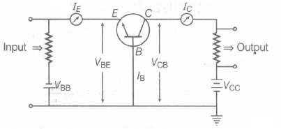
Working When input voltage, VBE is sufficient to make flow of emitter current, collector current flows in output circuit. In this condition, the circuit is said to be in active state.
The small change in VEB' produces sufficient change in emitter current and hence, in collector current. The input circuit offers very small resistance as ample change in emitter current occurs corresponding to small change in input voltage.
This lead to produce large change in output voltage inspite of smaller change in collector current (IE < IC) This shows that output circuit offer high resistance.
23.
(a) The values exhibited by sanjay are :
(i) Presence of mind
(ii) High degree of general awareness.
(b) (i) n - type ,
(ii) \(4\times 10^{ 4 }/m^{ 3 }\) ,
(iii) Energy gap decreases with doping
Here,\({ n }_{ i }=6\times 10^{ 8 }m^{ -3 };{ n }_{ e }=9\times 10^{ 12 }m^{ -3 }\)
\(\\ { n }_{ h }=\frac { { n }_{ i }^{ 2 } }{ { n }_{ e } } =\frac { \left( 6\times 10^{ 8 } \right) ^{ 2 } }{ 9\times 10^{ 12 } } =4\times 10^{ 4 }m^{ -3 }\)
As, after doping, \({ n }_{ e }>{ n }_{ h }\) so the new semiconductors is \(n\)-type. Energy gap decreases with doping.
24.
(i) (b) : \(E=\frac{V_{B}}{d}=\frac{0.4}{4.0 \times 10^{-7}}=1.0 \times 10^{6} \mathrm{Vm}^{-1}\)
(ii) (c) : Potential difference across = R = 3 - 0.4 = 2.6 V
\(\text { Resistance } R=\frac{\text { Potential difference }}{\text { Current }}\)
\(=\frac{2.6}{20 \times 10^{-3}}=130 \Omega\)
(iii) (d)
(iv) (b) : When the voltage will be the same that of the potential barrier disappears resulting in flow of current.
(v) (a) : \(\frac{1}{2} m v_{1}^{2}=e V_{B}+\frac{1}{2} m v_{2}^{2}\)
\(\Rightarrow \frac{1}{2} \times\left(9.1 \times 10^{-31}\right) \times\left(4 \times 10^{5}\right)^{2}\)
\(=1.6 \times 10^{-19} \times(0.4)+\frac{1}{2} \times 9.1 \times 10^{-31} \times v_{2}^{2}\)
On solving, we get
\(v_{2}=1.39 \times 10^{5} \mathrm{~m} \mathrm{~s}^{-1}\)
25.
(i) (c) :In insulator, energy band gap is > 3 eV
(ii) (b) : In conductor, separation between conduction and valence bands is zero and in insulator, it is greater than 1 eV. Hence in semiconductor the separation between conduction and valence band is 1 eV.
(iii) (a): According to band theory the forbidden gap in conductors Eg = 0, in insulators Eg > 3 eV and in semiconductors Eg < 3 eV.
(iv) (a): The four valence electrons of C, Si and Ge lie respectively in the second, third and fourth orbit.Hence energy required to take out an electron from these atoms (i.e. ionisation energy Eg) will be least for Ge, followed by Si and highest for C. Hence, the number of free electrons for conduction in Ge and Si are significant but negligibly small for C.
(v) (b)

12th Standard CBSE Syllabus & Materials
12th Standard CBSE
CBSE 12th Computer Science Python Revision Tour I - New Previous year Question Papers Study Material - QB365 Set A
NEW12th Standard CBSE
CBSE 12th Business Studies Planning Important Questions And Answers Study Material - QB365 Set A
NEW12th Standard CBSE
CBSE 12th Business Studies Business Environment Important Questions And Answers Study Material - QB365 Set A
NEW12th Standard CBSE
CBSE 12th Business Studies Principles of Management Important Questions And Answers Study Material - QB365 Set A



NCERT Books

Syllabus

Exam Pattern

Sample Question Papers

Previous year Question Papers

Important Notes

MCQ Practice test

NCERT Exemplers

Case study Questions

Image Based Questions

Passage based Questions

HOT Questions

Value Based Questions

Model Questions Papers
NCERT ( Book Back ) Questions

Assertion and Reason
Important Questions And Answers

CBSE 12th Standard CBSE Subjects
CBSE Standards