100% FREE ACCESS
12th Standard CBSE Syllabus & Materials
12th Standard CBSE
CBSE 12th Economics Government Budget and the Economy Previous year Question Papers Study Material - QB365 Set A
NEW12th Standard CBSE
CBSE 12th Computer Science Interface Python with MySQL - New Previous year Question Papers Study Material - QB365 Set A
NEW12th Standard CBSE
CBSE 12th Computer Science Database Concept - New Previous year Question Papers Study Material - QB365 Set A
NEW12th Standard CBSE
CBSE 12th Computer Science Data Communication - New Previous year Question Papers Study Material - QB365 Set A
NEW12th Standard CBSE
CBSE 12th Computer Science Data Structures - New Previous year Question Papers Study Material - QB365 Set A
NEW12th Standard CBSE
CBSE 12th Computer Science Functions - New Previous year Question Papers Study Material - QB365 Set A

Published on: 25/10/2025
Download CBSE Class 12th Standard CBSE Physics question papers, sample papers, important questions, and previous year solved papers in PDF format. Get free study materials, NCERT solutions, and exam preparation resources for Class 12th Standard CBSE Physics
Questions + Answers key
Take MCQ Physics Test
1.
It is found experimentally that 13.6 eV energy is required to separate a hydrogen atom into a proton and an electron. Compute the orbital radius and the velocity of the electron in a hydrogen atom.
2.
What is the force between two small charged spheres having charges of 2 x 10⁻⁷C and 3 x 10⁻⁷C placed 30 cm apart in air?
3.
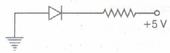
(i) In the following diagram, is the junction diode forward biased or reverse biased?
(ii) Draw the circuit diagram of a full wave rectifier and state how it works?
4.
Draw a schematic arrangement of the Geiger-Marsden experiment for studying a-particle scattering by a thin foil of gold. Describe briefly by drawing trajectories of the scattered a-particles. How can this study be used to estimate the size of the nucleus?
5.
Distinguish between a conductor, a semiconductor and an insulator on the basis of energy band diagrams.
6.
Use Gauss' law to derive the expression for the electric field between two uniformly charge parallel sheets with surface charge densities \(\sigma\) and -\(\sigma \) respectively.
7.
Three capacitors of 10, 15 and 30\(\mu F\) are connected in series and on this combination, a potential difference of 60V is applied. Calculate the charge, potential difference and energy stored on each capacitor.
8.
Two point charges of +16\(\mu C\) and \(-9\mu C\) are placed 8 cm apart in air. Determine the position of the point at which the resultant electric field is zero.
9.
What is the force between two small charged spheres having charges of 2 \(\times\) 10-7C and 3 \(\times\) 10-7C placed 30 cm apart in air?
10.
Draw equipotential surface for an electric dipole.
11.
Define the term electric dipole moment. Is it a scalar or a vector quantity?
12.
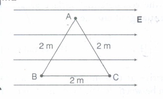
In uniform electric field, E = 10 NC-1 as shown in figure.
Find
(i) VA - VB (ii) VB - Vc
13.
A box encloses an electrical dipole consisting of charge 5\(\mu\)C and -5\(\mu\)C and of length 10 cm. What is the total electric flux through the box?
14.
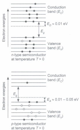
Draw energy band diagrams of n-type and p-type semiconductors at temperature T > 0 K Mark the donor and acceptor energy levels with their energies.
15.
Distinguish between intrinsic semiconductor and \(p\)-type semiconductor. Give reason, why a \(p\)-type semiconductor crystal is electrically neutral, although \(n_{ h }>>n_{ e }\) ?
16.
As per Bohr model, the minimum energy (in eV) required to remove an electron from the ground state of double ionized Li atom (Z = 3) is
1.51 eV
13.6 eV
40.8 eV
122.4 eV
17.
A capacitor is charged by using a battery which is then disconnected. A dielectric slab is then slipped between the plates, which results in
reduction of charge on the plates and increase of potential difference across the plates.
increase in the potential difference across the plate, reduction in stored energy, but no change in the charge on the plates.
decrease in the potential difference across the plates, reduction in the stored energy, but no change in the charge on the plates
none of these
18.
A capacitor is charged by a battery. The battery is removed and another identical uncharged capacitor is connected in parallel. The total electrostatic energy of resulting system
increases by a factor of 4
decreases by a factor of 2
remains the same
increases by a factor of 2
19.
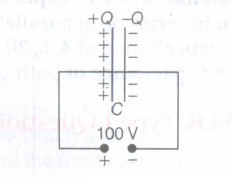
A 900 pF capacitor is charged by 100 V battery in the figure. How much electrostatic energy is stored by the capacitor?
45 x 10-6 J
4.5 x 10⁶ J
4.5 x 10⁻⁶ J
0.45 x 10⁵ J
20.
If electrostatic potential at the surface of a sphere of 5 cm radius is 50 V,then the potential at the centre of sphere will be
10 V
50 V
250 V
zero
21.
If the orbital radius of the electron in a hydrogen atom is 4.7 x 10⁻¹¹ m. Compute the kinetic energy of the electron in hydrogen atom.
15.3eV
- 15.3eV
13.6 eV
-13.6 eV
22.
Three charges each equal to +2 C are placed at the corners of an equilateral triangle. If the force between any two charges be F, then the net force on either will be
3F
2F
√2F
√3F
23.
Two charges of 2μ C and 5μ C are placed 2.5 cm apart. The ratio of the Coulomb's force experienced by them is:
1:1
2:5
√2:√5
4:25
24.
A condenser is charged to double its initial potential. The energy stored in the condenser becomes x times, where x =
2
4
1
1/2
25.
Mobilities of electrons and holes in a sample of intrinsic germanium at room temperature are \(0.36{ m }^{ 2 }{ v }^{ -1 }s^{ -1 } \ and \ 0.17 \ { m }^{ 2 }{ v }^{ -1 }s^{ -1 }\)The electron and hole densities are each equal to \(2.5 \times 10^{ 19 }m^{ -3 }\) .The electrical conductivity of germanium is
0.47 \(Sm^{ -1 }\)
1.09 \(Sm^{ -1 }\)
2.12 \(Sm^{ -1 }\)
4.24 \(Sm^{ -1 }\)
26.
Charge on a body which carries 200 excess electrons is
\(-3.2\times 10^{-18}C\)
\(9\times10^{-9}Nm^2C^{-2}\)
\(3.2\times 10^{-17}C\)
\(3.2\times 10^{-17}C\)
27.
In an unbiased p-n junction, holes diffuse from the p- region to n- region because
Free electrons in the n-region attract them
they move across the junction by the potential difference
hole concentration in p-region is more as compared to hole concentration in n-region
all the above
28.
(i) Two point charges q1, and q2, are kept at a distance of r12 in air. Deduce the expression for the electrostatic potential energy of this system.
(ii) If an external electric field (E) is applied on the system, write the expression for the total energy of this system.
29.
In a Geiger-Marsden experiment, what is the distance of closest approach to the nucleus of a 7.7 MeV \(\alpha\)-particle before it comes momentarily to rest and reverses its direction?
30.
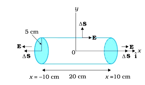
An electric field is uniform, and in the positive x direction for positive x, and uniform with the same magnitude but in the negative x direction for negative x. It is given that E = 200 \(\hat{i}\) N/C for x > 0 and E = –200 \(\hat{i}\) N/C for x < 0. A right circular cylinder of length 20 cm and radius 5 cm has its centre at the origin and its axis along the x-axis so that one face is at x = +10 cm and the other is at x = –10 cm (Fig.)
(a) What is the net outward flux through each flat face?
(b) What is the flux through the side of the cylinder?
(c) What is the net outward flux through the cylinder?
(d) What is the net charge inside the cylinder.
31.
(a) Draw the circuit arrangement for studying the V - I characteristics of a p-n junction diode in (i) forward and (ii) reverse bias. Briefly explain how the typical V - I characteristics of a diode are obtained and draw these characteristics.
(b) With the help of necessary circuit diagram explain the working ot a photo diode used for detecting optical signals.
32.
(a) Explain with the help of a diagram, how a depletion layer and barrier potential are formed in a junction diode
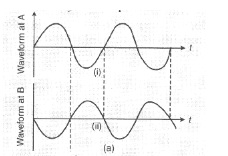
(b) Draw a circuit diagram of full wave rectifier. Explain its working and draw input and output waveforms full wave rectifier. Explain its working and draw input and output waveforms
33.
(a) Define electric dipole moment. Is it a scalar or a vector? Derive the expression for the electric field of a dipole at a point on the equatorial plane of the dipole.
(b) Draw the equipotential surfaces due to an electric dipole. Locate the points where the potential due to the dipole is zero.
34.
A uniformly charged conducting sphere 2.4m diameter has a surface charge density of 180.0 \(\mu C/m^2\)
(i) Find the charge on the sphere.
(ii) What is the total flux leaving the surface of the sphere?
35.
36.
37.
Assertion (A) : The resistivity of a semiconductor increases with temperature.
Reason (R) : The atoms of a semiconductor vibrate with larger amplitude at higher temperatures thereby increasing its resistivity.
Codes:
(a) Both A and R are true and R is the correct explanation of A
(b) Both A and R are true but R is NOT the correct explanation of A
(c) A is true but R is false
(d) A is false and R is also false
38.
Assertion (A) : Capacity of a parallel plate capacitor increases when distance between the plates is decreased.
Reason (R) : Capacitance of capacitor is inversely proportional to distance between them.
Codes:
(a) Both A and R are true and R is the correct explanation of A
(b) Both A and R are true but R is NOT the correct explanation of A
(c) A is true but R is false
(d) A is false and R is also false
39.
40.
When an insulator is placed in an external field, the dipoles become aligned. Induced surface charges on the insulator establish a polarization field Ēi in its interior. The net field Ē in the insulator is the vector sum of Ē, and Ēi as shown in the figure.

In the application of an external electric field, the effect of aligning the electric dipoles in the insulator is called polarization, and the field Ē; is known as the polarisation field. The dipole moment per unit volume of the dielectric is known as polarisation (P). For linear isotropic dielectrics, P =χE, where χ = electrical susceptibility of the dielectric medium.
(i) Which among the following is an example of a polar molecule?
(2)O₂
(b)H
(c)N2
(d) HCI
(ii) When air is replaced by a dielectric medium of constant K, the maximum force of attraction between two charges separated by a distance
(a)increases K times
(b) remains unchanged
(c) decreases K times
(d) increases 2K times.
(iii) Which of the following is a dielectric?
(a) Copper
(b) Glass
(c) Antimony (Sb)
(d) None of these
(iv) For a polar molecule, which of the following statements is true ?
(a) The centre of gravity of electrons and protons coincide.
(b) The centre of gravity of electrons and protons do not coincide.
(c) The charge distribution is always symmetrical.
(d) The dipole moment is always zero.
(v) When a comb rubbed with dry hair attracts pieces of paper. This is because the
(a) comb polarizes the piece of paper
(b) comb induces a net dipole moment opposite to the direction of field
(c) electric field due to the comb is uniform
(d) comb induces a net dipole moment perpendicular to the direction of field
1.
Total energy of the electron in hydrogen atom is –13.6 eV = –13.6 × 1.6 × 10–19 J = –2.2 ×10⁻¹⁸ J. Thus from Equation we have
\(-\frac{e^{2}}{8 \pi \varepsilon_{0} r}=-2.2 \times 10^{-18} \mathrm{~J}\)
This gives the orbital radius
\(r=-\frac{e^{2}}{8 \pi \varepsilon_{0} E}=-\frac{\left(9 \times 10^{9} \mathrm{~N} \mathrm{~m}^{2} / \mathrm{C}^{2}\right)\left(1.6 \times 10^{-19} \mathrm{C}\right)^{2}}{(2)\left(-2.2 \times 10^{-18} \mathrm{~J}\right)}\)
= 5.3 × 10⁻¹¹ m
The velocity of the revolving electron can be computed from Eq.uation with m = 9.1 × 10⁻³¹ kg,
\(v=\frac{e}{\sqrt{4 \pi \varepsilon_{0} m r}}=2.2 \times 10^{6} \mathrm{~m} / \mathrm{s}\)
2.
Repulsive force of magnitude 6 x 10⁻³ N
Charge on the first sphere, q1 = 2 x 10⁻⁷ C
Charge on the second sphere, q2 = 3 x 10⁻⁷ C
Distance between the spheres, r = 30 cm = 0.3 m
Electrostatic force between the spheres is given by the relation,
\(F=\frac{q_{1} q_{2}}{4 \pi \in_{0} r^{2}}\)
Where, ∈0 = Permittivity of free space
\(\frac{1}{4 \pi \in_{0}}=9 \times 10^{9} N m^{2} C^{-2}\)
\(F=\frac{9 \times 10^{9} \times 2 \times 10^{-7} \times 3 \times 10^{-7}}{(0.3)^{2}}=6 \times 10^{-3} N\)
Hence, force between the two small charged spheres is 6 x 10⁻³ N. The charges are of same nature. Hence, force between them will be repulsive.
3.
The given diagram shown below
.png)
The circuit above can be redrawn as follows
.png)
As the p-section is connected to negative terminal of the battery, the diode shown is reverse biased.
(ii) During the first half of input cycle, the upper end of the coil is at positive potential and lower end at negative potential. The function diode DI is forward biased and D2 in reverse biased. Current flows in output load in the
direction shown in figure. During the second half of input cycle, D2 is forward biased. In this way, current flows in the load in the single direction as shown in figure.
.png)
4.
Given figure shows a schematic diagram of Geiger -Marsden experiment.
s.png)
s.png)
The size of the nucleus can be obtained by finding impact parameter b using trajectories of n-particle. The impact parameter is the perpendicular distance of the initial velocity vector of o-particle from the central line of nucleus when it is far away from the atom.
Rutherford calculated impact parameter as
\(b=\frac { 1 }{ 4\pi { \varepsilon }_{ 0 } } .\frac { Z{ e }^{ 2 }\cot { \left( { \theta }/{ 2 } \right) } }{ E } \)
where,
E = KE of (\(\alpha\) -particle)
\(\theta\) = scattering angle
Z = atomic number of atom
The size of the nucleus is smaller than the impact parameter.
The idea of the size of the nucleus can also be obtained by finding the distance of closest approach.
5.
.png)
(a) metals, (b) insulators and (c) semiconductors
Two distinguishing features:
(i) In conductors, the valence band and conduction band tend to overlap (or nearly overlap) while in insulators they are separated by a large energy gap and in semiconductors they are separated by a smaJ1'ep.ergygap.
(ii) The conduction band, of a conductor, has a large number of electrons available for electrical conduction. However the conduction band of insulators is almost empty while that of the semiconductor has only a (very) small number of such electrons available for electrical conduction.
.png)
6.
Let us consider two uniformly charge parallel sheets carrying surface charge densities + \(\sigma \) and -\(\sigma \) respectively and are separated by a small distance from each other.
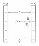
By Gauss' law, it can be proved that, electric field intensity due to a uniformly charged infinite plane sheet as nearby is given by
E = \(\frac { \sigma }{ 2{ \varepsilon }_{ 0 } } \) ....(i)
The electric field is directed normally outward from the plane sheet, if nature of charge on sheet is positive and normally inward, if charge is of negative nature. Let \(\widehat { r } \) represents unit vector directed from positive plate to negative plate.
Now, electric field intensity (EFI) at any point P between the two plates is given by
(i) E1 = + \(\frac { \sigma }{ 2{ \varepsilon }_{ 0 } } \widehat { r } \) [due to positive plate]
(ii) E2 = + \(\frac { \sigma }{ 2{ \varepsilon }_{ 0 } } \widehat { r } \) [due to negative plate]
\(\therefore\) New EFI at point P,
E = E1 + E2
= \(\frac { \sigma }{ 2{ \varepsilon }_{ 0 } } \widehat { r } +\frac { \sigma }{ 2{ \varepsilon }_{ 0 } } \widehat { r } \)
\(\Rightarrow\) E = \(\frac { \sigma }{ { \varepsilon }_{ 0 } } \widehat { r } \)
Thus, uniform electric field is produced between the two infinite parallel plane sheet of charge which is directed from positive plate to negative plate.
7.
Let the equivalent capacitance of the series combination be C. Then,
\(\frac { 1 }{ C } =\frac { 1 }{ { { C }_{ 1 } } } +\frac { 1 }{ { C }_{ 2 } } +\frac { 1 }{ { C }_{ 3 } } =\frac { 1 }{ 10 } +\frac { 1 }{ 15 } +\frac { 1 }{ 30 } F\)
\( =\frac { 3+2+1 }{ 30 } =\frac { 6 }{ 30 } =\frac { 1 }{ 5 } \Rightarrow C=5\mu \)
Charge stored on the combination is
q = CV = 5 x 60 = 300\(\mu C\)
Since, the capacitor are in series, the charge on each capacitor is 300\(\mu C\).
The potential difference across the three capacitors are
\({ V }_{ 1 }=\frac { q }{ { C }_{ 1 } } =\frac { 300 }{ 10 } =30V\)
\(\\ { V }_{ 2 }=\frac { q }{ { C }_{ 2 } } =\frac { 300 }{ 15 } =20V\)
\(\\ { V }_{ 3 }=\frac { q }{ { C }_{ 3 } } =\frac { 300 }{ 30 } =10V\)
Energy of the capacitors are
\({ U }_{ 1 }=\frac { 1 }{ 2 } q{ V }_{ 1 }=\frac { 1 }{ 2 } \times 300\times 30=4500\mu J\)
\(\\ { U }_{ 2 }=\frac { 1 }{ 2 } q{ V }_{ 2 }=\frac { 1 }{ 2 } \times 300\times 20=3000\mu J\)
\(\\ { U }_{ 3 }=\frac { 1 }{ 2 } q{ V }_{ 3 }=\frac { 1 }{ 2 } \times 300\times 10=1500\mu J\)
8.
Let E = 0 at a distance x to the right of \(-9\mu C\) charge.
Use k\({q_1\times1\over(8+x)^2}={kq_2\times 1\over x^2}\)
9.
Given q1 = 2 \(\times\) 10-7 C, q2 = 3 \(\times\) 10-7 C r = 30 cm = 0.3 m
Therefore, Force of repulsion, F = 9 \(\times\) 109 \(\times\) \(\frac { { q }_{ 1 }{ q }_{ 2 } }{ { r }^{ 2 } } \)
= \(9\times { 10 }^{ 9 }\times \frac { 2\times { 1 }0^{ -7 }\times 3\times { 10 }^{ -7 } }{ { (0.3) }^{ 2 } } =\frac { 54\times { 10 }^{ -5 } }{ 9\times { 10 }^{ -2 } } \)
\(=\ 6\times { 10 }^{ -3 }N\)
10.
The equipotential surfaces for an electric dipole are as shown below in the figure by dotted Iines.
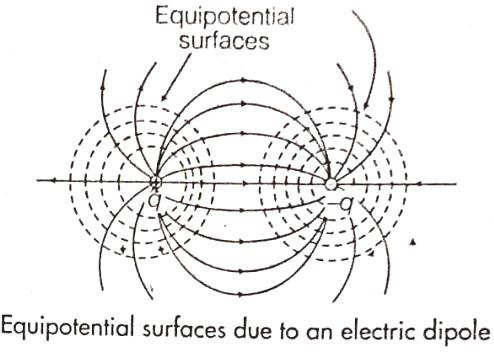
Electric field is always perpendicular to an equipotential surface and as a result, work done in moving a charge between two points On an equipotential surface is zero.
11.
The product of the magnitude of one of the point charges constituting an electric dipole and the separation between them is termed as electric dipole moment. It is a vector quantity.
12.
Since, electric field is directed from higher electric potential to lower electric potential,
(i) Thus, VB> VA , so VA - VB will be negative
Further, dAB = 2 cos 60° = 1m
\(\therefore\) VA - VB = - EdAB = (-10)(1) = -10 V
(ii) As, VB > VC so VB - Vc will be positive
Further, dBC = 2.0 m
\(\therefore\) VB - Vc = (10) (2) = 20 V
13.
Since, an electric dipole consists of two equal and opposite charges, the net charge on the dipole is zero.
Hence, the net electric flux coming out of the closed surface of the box or through the box is zero.
14.
15.
In a pure semiconductors (Ge or Si) called intrinsic semiconductor the electrically conductivity is related by the electrons thermally excited from the valence band to the conduction band. There are equal number densities of free electrons and holes in conduction band and valence band of intrinsic semiconductor.
When a pure semiconductor of Ge or Si is doped with impurity atoms of valence three (like B or A1), some additional energy levels are created just above the upper energy level of valence band. Due to it, band gap of \(p\)-type semiconductor becomes smaller than intrinsic semiconductor. Also in \(p\)-type semiconductor, the number density of holes is more than that of electrons.
A \(p\)-type semiconductor is obtained when a trivalent atoms (Bor A1) are doped in pure semiconductor of Ge or Si. Here each doped trivalent atom shares its three valence electrons with the three atoms of Ge or Si and form bonds. While the fourth bond remains unbounded. Due to it, a hole is created. Since the impurity atoms and atoms of semiconductor are electrically neutral, hence \(p\)-type semiconductor is also neutral.
16.
(d)
122.4 eV
17.
(c)
decrease in the potential difference across the plates, reduction in the stored energy, but no change in the charge on the plates
18.
(b)
decreases by a factor of 2
19.
(c)
4.5 x 10⁻⁶ J
20.
(b)
50 V
21.
(a)
15.3eV
22.
(d)
√3F
23.
(a)
1:1
24.
(b)
4
25.
(c)
2.12 \(Sm^{ -1 }\)
26.
(c)
\(3.2\times 10^{-17}C\)
27.
(c)
hole concentration in p-region is more as compared to hole concentration in n-region
28.
Work done in bringing q2 from infinity to a point
\(=q_2 \times \frac{1}{4 \pi \epsilon_0} \frac{q_1}{r_{12}}\)
The potential energy of the system
\(=\frac{1}{4 \pi \epsilon_0} \frac{q_1 q_2}{r_{12}}\)
b) Total energy of the system
\(=q_1 V_1+q_2 V_2+\frac{1}{4 \pi \epsilon_0} \frac{q_1 q_2}{r_{12}}\)
29.
The key idea here is that throughout the scattering process, the total mechanical energy of the system consisting of an\(\alpha\) -particle and a gold nucleus is conserved. The system’s initial mechanical energy is Et, before the particle and nucleus interact, and it is equal to its mechanical energy Ef when the (-particle momentarily stops. The initial energy Et is just the kinetic energy K of the incoming \(\alpha\)- particle. The final energy Ef is just the electric potential energy U of the system. The potential energy U can be calculated from equation.
Let d be the centre-to-centre distance between the (-particle and the gold nucleus when the (-particle is at its stopping point. Then we can write the conservation of energy Et = Ef as
\(K=\frac{1}{4 \pi \varepsilon_{0}} \frac{(2 e)(Z e)}{d}=\frac{2 Z e^{2}}{4 \pi \varepsilon_{0} d}\)
Thus the distance of closest approach d is given by
\(d=\frac{2 Z e^{2}}{4 \pi \varepsilon_{0} K}\)
The maximum kinetic energy found in\(\alpha\) -particles of natural origin is 7.7 MeV or 1.2 × 10⁻¹² J. Since 1/4 \(\pi\) E0= 9.0 × 10⁹ N m2/C2. Therefore with e = 1.6 × 10⁻¹⁹ C, we have
\(d=\frac{(2)\left(9.0 \times 10^{9} \mathrm{Nm}^{2} / \mathrm{C}^{2}\right)\left(1.6 \times 10^{-19} \mathrm{C}\right)^{2} \mathrm{Z}}{1.2 \times 10^{-12} \mathrm{~J}}\)
= 3.84 × 10⁻¹⁶ Z m
The atomic number of foil material gold is Z = 79, so that d (Au) = 3.0 × 10⁻¹⁴ m = 30 fm. (1 fm (i.e. fermi) = 10–15 m.)
The radius of gold nucleus is, therefore, less than 3.0 × 10⁻¹⁴ m. This is not in very good agreement with the observed result as the actual radius of gold nucleus is 6 fm. The cause of discrepancy is that the distance of closest approach is considerably larger than the sum of the radii of the gold nucleus and the \(\alpha\)-particle. Thus, the \(\alpha\)-particle reverses its motion without ever actually touching the gold nucleus.
30.
(a) We can see from the figure that on the left face E and ΔS are parallel. Therefore, the outward flux is
φL= E.ΔS = – 200 \(\hat{i}\). ΔS
= + 200 ΔS, since\(\hat{i}\) . ΔS = – ΔS
= + 200 x \(\pi \) (0.05)2 = + 1.57 N m2 C–1
On the right face, E and ΔS are parallel and therefore φR = E.ΔS = + 1.57 N m2 C–1
(b) For any point on the side of the cylinder E is perpendicular to ΔS and hence E.ΔS = 0. Therefore, the flux out of the side of the cylinder is zero
(c) Net outward flux through the cylinder
φ = 1.57 + 1.57 + 0 = 3.14 N m2 C–1
(d) The net charge within the cylinder can be found by using Gauss’s law which gives
q = ε0φ
= 3.14 x 8.854 × 10–12 C
= 2.78 x 10⁻¹¹ C
31.
.png)
Reverse biasing
.png)
The VI characteristics are obtained by connecting the battery, to the diode, through a potentiometer (or rheostat). The applied voltage to the diode is changed. The values of current, for different values of voltage, are noted and a graph between V and I is plotted. The V-I characteristics, of a diode, have the form shown here.
.png)
(b) The circuit diagram, for the photodiode, is shown here.
.png)
The photodiode is illuminated by optical signal, whose photon energy is greater than the energy gap of the semiconductor used.
The electric field, at the junction, separates the electrons and holes and thus gives rise to an emf.
When an external load is connected, a (photo) current flows through it. The magnitude of this current is proportional to the intensity of light incident on the photodiode.
32.
.png)
(a) Due to the diffusion of electrons and the holes, from their majority zone to minority zone, a layer of positive and negative space charge region on either side on the junction is formed. This is called the depletion region.
The loss of electrons, from n-region and gain of electrons by the p-region, causes a difference of potential across the junction. This tends to prevent the movement of charge carriers across the junction and is, therefore, termed as barrier potential.
.png)
For positive half cycle of input ac, one of the two diodes gets forward biased and conducts and output current is obtained across the load RL, For negative half cycle of input ac, the other diode
gets forward biased and thus output current is obtained due to it. Therefore, output is obtained for both the cycles of input ac.
.png)
33.
(a) Electric dipole moment : The strength of an electric dipole is measured by the quantity electric dipole moment. Its magnitude is equal to the product of the magnitude of either charge and the distance between the two charges.
Electric dipole moment, p = q x d
It is a vector quantity.
In vector form, it is written as \(\overrightarrow{p}\) = q x 2 \(\overrightarrow{a}\)\(\hat{p}\)where direction of 2 \(\overrightarrow{a}\) \(\hat{p}\) is from negative charge to positive charge.
Electric field of dipole at points on the equatorial plane :
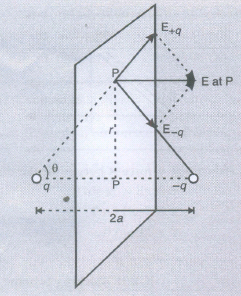
The magnitudes of the electric field due to the two charges +q and -q are given by,
\(E_{+q} = \frac{q}{4\pi\epsilon_0}\frac{1}{(r^2+a^2)}\) ..........(i)
\(E_{-q} = \frac{q}{4\pi\epsilon_0}\frac{1}{(r^2+a^2)}\) .............(ii)
\(\therefore\) E+q = E-q
The direction of E+ q and E-q are as shown in the figure. The components normal to the dipole axis cancel away. The components along the dipole axis add up.
\(\therefore\) Total electric field E = - (E+q+ E_q ) cos q \(\hat{p}\)
[ Negative sign shows that field is opposite to \(\hat{p}\) ]
\(E = \frac{-2qa}{4\pi\epsilon_0(r^2+a^2)^{3/2}}\hat{p}\) ............(iii)
At large distances (r > > a), this reduces to
\(E = \frac{2qa}{4\pi\epsilon_0r^3}\hat{p}\) .................(iv)
= 2qa\(\hat{p}\)
\(\therefore\) = \(\overrightarrow{p}\)
\(\therefore\) \(E = \frac{-\overrightarrow{p}}{4\pi\epsilon_0r^3}\) ( r > > a )
(b) Equipotential surface due to electric dipole:
.png)
The potential due to the dipole is zero at the line bisecting the dipole length
34.
Here, \(R={2.4\over 2}=1.2m\)
\(\sigma=180.0 \mu C/m^2=180\times 10^{-6}Cm^{-2}\)
(i) Charge on the sphere q= \(4\pi R^2\sigma\)
\(=4\times 3.14\times(1.2)^2\times 180\times 10^{-6}\)
\(3.53\times 10^{-3}C\)
Electric flux, \(\phi_E={q\over \epsilon_o}={3.53\times10^{-3}\over8.85\times10^{-12}}\)
35.
36.
37.
(d) : With the increase of temperature, the average energy exchanged in a collision increases and so more valence electrons can cross the energy gap, thereby increasing the electron-hole pairs. As in a semiconductor, conduction occurs mainly through electron-hole pairs, so conductivity increases with increase of temperature. Which in turn implies that the resistivity of a semiconductor decreases with rise in temperature.
38.
(a): Capacitance of parallel plate capacitor is \(C=\frac{\varepsilon_{0} A}{d}\) Thus distance decreases and capacitance of capacitor increases.
39.
40.

12th Standard CBSE Syllabus & Materials
12th Standard CBSE
CBSE 12th Computer Science Python Revision Tour I - New Previous year Question Papers Study Material - QB365 Set A
NEW12th Standard CBSE
CBSE 12th Business Studies Planning Important Questions And Answers Study Material - QB365 Set A
NEW12th Standard CBSE
CBSE 12th Business Studies Business Environment Important Questions And Answers Study Material - QB365 Set A
NEW12th Standard CBSE
CBSE 12th Business Studies Principles of Management Important Questions And Answers Study Material - QB365 Set A



NCERT Books

Syllabus

Exam Pattern

Sample Question Papers

Previous year Question Papers

Important Notes

MCQ Practice test

NCERT Exemplers

Case study Questions

Image Based Questions

Passage based Questions

HOT Questions

Value Based Questions

Model Questions Papers
NCERT ( Book Back ) Questions

Assertion and Reason
Important Questions And Answers

CBSE 12th Standard CBSE Subjects
CBSE Standards