100% FREE ACCESS
12th Standard CBSE Syllabus & Materials
12th Standard CBSE
CBSE 12th Economics Government Budget and the Economy Previous year Question Papers Study Material - QB365 Set A
NEW12th Standard CBSE
CBSE 12th Computer Science Interface Python with MySQL - New Previous year Question Papers Study Material - QB365 Set A
NEW12th Standard CBSE
CBSE 12th Computer Science Database Concept - New Previous year Question Papers Study Material - QB365 Set A
NEW12th Standard CBSE
CBSE 12th Computer Science Data Communication - New Previous year Question Papers Study Material - QB365 Set A
NEW12th Standard CBSE
CBSE 12th Computer Science Data Structures - New Previous year Question Papers Study Material - QB365 Set A
NEW12th Standard CBSE
CBSE 12th Computer Science Functions - New Previous year Question Papers Study Material - QB365 Set A

Published on: 25/10/2025
Download CBSE Class 12th Standard CBSE Physics question papers, sample papers, important questions, and previous year solved papers in PDF format. Get free study materials, NCERT solutions, and exam preparation resources for Class 12th Standard CBSE Physics
Questions + Answers key
Take MCQ Physics Test
1.
State Kirchhoff's rules. Explain briefly how these rules are justified.
2.
A negligibly small current is passed through a wire length 15 m and uniform cross-section \(6.0\times { 10 }^{ -7 }m^{ 2 }\) and its resistance is measured to be \(5.0\Omega \). What is the resistivity of the material at the temperature of the experiment?
3.
A uniform wire is cut into four segments. Each segment is twice as long as the earlier segment. If the shortest segment has a resistance of \(2 \ \Omega\), find the resistance of original wire.
4.
Distinguish between intrinsic semiconductor and \(p\)-type semiconductor. Give reason, why a \(p\)-type semiconductor crystal is electrically neutral, although \(n_{ h }>>n_{ e }\) ?
5.
Suppose a pure Si crystal has \(5\times 10^{ 28 }\) atmos \(m^{ -3 }\). It is doped by ppm concentration of pentavalent As. Calculate the number of electrons and holes. Given that \({ n }_{ i }=1.5\times { 10 }^{ 16 }m^{ 3 }\)
6.
Two identical cells of e.m.f 1.5V each joined in parallel provide supply to an external circuit consisting of two resistors of 17\(\Omega\) each joined in parallel. A very high resistance voltmeter reads the terminal voltage of the cells to be 1.4V. What is the internal resistance of each cell?
7.
E.M.F of a cell is 1.5V and its internal resistance 1\(\Omega\) . For what current drawn from the cell will its terminal potential difference be half of its e.m.f?
8.
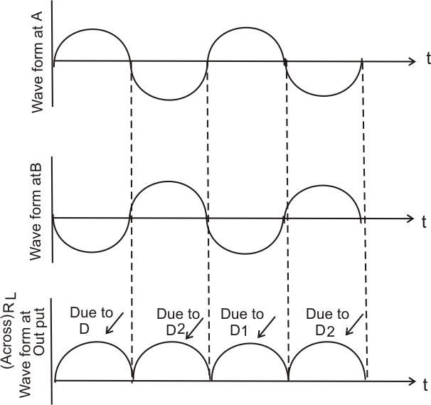
Draw the circuit diagram of a full wave rectifier. Explain its working principle. Show the input waveforms given to the diodes D1 and D2 and the corresponding output waveforms obtained at the load connected to the circuit.
9.
Draw the energy band diagrams of
(i) n-type and
(ii) p-type semiconductor at temperature, T> OK.
In the case n-type Si semiconductor, the donor energy level is slightly below the bottom of conduction band whereas in p-type semiconductor, the acceptor energy level is slightly above the top of the valence band. Explain, what role do these energy levels play in conduction and valence bands.
10.
(i) Distinguish between n-type and p-type semiconductors on the basis of energy band diagrams.
(ii) Compare their conductivities at absolute zero temperature and at room temperature
11.
Two cells of emf E1, E2 and internal. resistances r1 and r2 respectively are connected in parallel as shown in the figure.
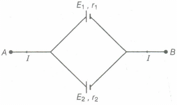
Deduce the expressions for
(i) the equivalent emf of the combination.
(ii) the equivalent resistance of the combination and
(iii) the potential difference between the points A and B.
12.
Define the terms
(i) drift velocity,
(ii) relaxation time.
A conductor of length L is connected to a de source of emf E. If this conductor is replaced by another conductor of same material and same area of crosssection but of length 3 L, how will the drift velocity change?
13.
How many electrons pass through a wire in 2 minutes, if the current passing through wire is 300 mA?
14.
(a) Three resistors \(1\Omega ,2\Omega \ and\ 3\Omega \) are combined in series. What is the total resistance of the combination?
(b) If the combination is connected to a battery of emf 12 V and negligible internal resistance, obtain the potential drop across each resistor.
15.
In half-wave rectification, what is the output frequency, if the input frequency is 50 Hz? What is the output frequency of a full wave rectifier for the same input frequency?
16.
(a) Distinguish between an intrinsic semiconductor and a p-type semiconductor. Give reason why a p-type semiconductor crystal is electrically neutral, although nh >> ne.?
(b) Explain, how the heavy doping of both p- and n- sides of a p-n junction diode results in the electric field of the junction being extremely high even with a reverse bias voltage of a few volts. Explain, with the help of a circuit diagram, how this property is used in voltage regulator.
17.
(a) State Ohm's law.
(b) Define resistance. Give its SI unit.
18.
(a) Define electric current. What is its S.I. unit? Is it a scalar or a vector quantity? What is the direction of electric current?
(b) How many electrons flowing per second should flow to produce a current of 1A?
19.
An external resistance R is connected to a cell of internal resistance r.The current in the circuit is maximum when:
R > r
R < r
R = r
cannot be parallel
20.
A wire of resistance 3Ω is cut into there equal pieces, which are joined to from a triangle. The equivalent resistance between any two corners of the triangle is
\({3\over 2}Ω\)
\({2\over 3}Ω\)
\({1\over 4}Ω\)
4Ω
21.
Resistivity of a conductor depends upon its:
resistance
length
area of cross - section
none of the above characteristics
22.
Three equal resistors each of resistance R are connected so as to form a triangle. The equivalent resistance across any two corners is:
2R/3
R/3
3R/2
3R
23.
The equivalent resistance of n resistors each of same resistance when connected in parallel is Rp. If they are connected in series, the equivalent resistance will be:
Rp/n2
Rp/n
nRp
n2Rp
24.
When a current I is set up in a wire of radius r, the drift speed id vd. If the same current is set up through a wire of radius 2r the drift speed will be
vd/4
vd/2
2vd
4vd
25.
The number density of free electrons in the semiconductor is \(10^{ 158 }m^{ -3 }\). It is doped with a pentavalent impurity atoms of number density \(10^{ 24 }m^{ -3 }\) the number density of free electrons \(m^{ -3 }\) increases by a factor of
43
6
\({ 10 }^{ 6 }\)
\({ 10 }^{ 24 }\)
26.
The resistance of an intrinsic semi-conductor when heated
increases
remains constant
decreases linearly
decreases exponentially
27.
Carbon, silicon and germanium have four valence electrons each, These are characterised by valence and conduction bands separated by energy bandgap respectively equal to \((E_{ g })_{ c, }({ E }_{ g })_{ si }\ and\ { (E }_{ g })_{ Ge }\)Which of the following statements is true?
\((E_{ g })_{ si, }<({ E }_{ g })_{ Ge }<\ { (E }_{ g })_{ C }\)
\((E_{ g })_{ C, }>({ E }_{ g })_{ si }>\ { (E }_{ g })_{ Ge }\)
\((E_{ g })_{ C, }=({ E }_{ g })_{ si }=\ { (E }_{ g })_{ Ge }\)
\((E_{ g })_{ C, }=({ E }_{ g })_{ si }=\ { (E }_{ g })_{ Ge }\)
28.
The built in potential of p-n junction diode is a function of
temperature
biased voltage
doping density
all of the above
29.
n - type semiconductor is obtained when
germanium is doped with arsenic
germanium is doped with indium
germanium is doped with aluminium
silicon is doped with indium
30.
In good conductorsof electricity the type of bonding that exists is
ionic
vander waals
covalent
metallic
31.
From Bohr's atomic model, we know that the electrons have well defined energy levels in an isolated atom. But due to interatomic interactions in a crystal, the electrons of the outer shells are forced to have energies different from those in isolated atoms. Each energy level splits into a number of energy levels forming a continuous band.The gap between top of valence band and bottom of the conduction band in which no allowed energy levels for electrons can exist is called energy gap.
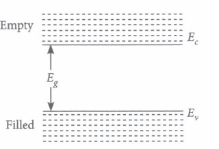
(i) In an insulator energy band gap is
| (a) Eg = 0 | (b) Eg< 3eV | (c) Eg > 3eV | (d) None of the above |
(ii) In a semiconductor, separation between conduction and valence band is of the order of
| (a) 0 eV | (b) 1 eV | (c) 10 eV | (d) 50 eV |
(iii) Based on the band theory of conductors, insulators and semiconductors, the forbidden gap is smallest in
| (a) conductors | (b) insulators | (c) semiconductors | (d) All of these |
(iv) Carbon, silicon and germanium have four valence electrons each. At room temperature which one of the following statements is most appropriate?
| (a) The number of free electrons for conduction is significant only in Si and Ge but small in C. |
| (b) The number of free conduction electrons is significant in C but small in Si and Ge. |
| (c) The number of free conduction electrons is negligibly small in all the three. |
| (d) The number offree electrons for conduction is significant in all the three. |
(v) Solids having highest energy level partially filled with electrons are
| (a) semiconductor | (b) conductor | (c) insulator | (d) none of these |
32.
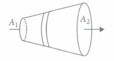
The flow of charge in a particular direction constitutes the electric current. Current is measured in Ampere. Quantitatively, electric current in a conductor across an area held perpendicular to the direction of flow of charge is defined as the amount of charge is flowing across that area per unit time.
Current density at a point in a conductor is the ratio of the current at that point in the conductor to the area of cross section of the conductor of that point.
The given figure shows a steady current flows in a metallic conductor of non uniform cross section. Current density depends inversely on area, so, here \(J_{1}>J_{2}, \text { as } A_{1}
(i) What is the current flowing through a conductor, if one million electrons are crossing in one millisecond through a cross-section of it ?
| (a) 2.5 x 10⁻¹⁰ A | (b) 1.6 x 10⁻¹⁰ A |
| (c) 7.5 X 10⁻⁹ A | (d) 8.2 x 10⁻¹¹ A |
(ii) SI unit of electric current is
| (a) Cs | (b) Ns-2 | (c) Cs-1 | C-1s-1 |
(iii) A steady current flows in a metallic conductor of non-uniform cross-section. Which of these quantities is constant along the conductor?
| (a) Electric field | (b) Drift velocity | (c) Current | (d) Current density |
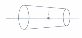
(iv) A constant current I is flowing along the length of a conductor of variable cross-section as shown in the figure. The quantity which does not depend upon the area of cross-section is
| (a) electron density | (b) current density |
| (c) drift velocity | (d) electric field |
(v) When a current of 40 A flows through a conductor of area 10 m2, then the current density is
| (a) 4 A/m2 | (b) 1 A/m2 | (c) 2 A/m2 | (d) 8 A/m2 |
33.
Assertion (A) : At absolute zero the conductivity of semiconductor is zero.
Reason (R) : In a semiconductor there are no free electrons at any temperature.
Codes:
(a) Both A and R are true and R is the correct explanation of A
(b) Both A and R are true but R is NOT the correct explanation of A
(c) A is true but R is false
(d) A is false and R is also false
34.
Assertion (A) : The depletion layer in the p-n junction is free from mobile charge carriers.
Reason (R) : There is no electric field across the junction barrier.
Codes:
(a) Both A and R are true and R is the correct explanation of A
(b) Both A and R are true but R is NOT the correct explanation of A
(c) A is true but R is false
(d) A is false and R is also false
35.
Assertion: The drift velocity of electrons in a metallic wire will decrease, if the temperature of the wire is increased.
Reason: On increasing temperature, conductance of metallic wire decreases.
Codes:
(a) Both A and R are true and R is the correct explanation of A
(b) Both A and R are true but R is NOT the correct explanation of A
(c) A is true but R is false
(d) A is false and R is also false
36.
Assertion: Current is a scalar quantity.
Reason: Electric current arises due to continuous flow of charged particles or ions.
Codes:
(a) Both A and R are true and R is the correct explanation of A
(b) Both A and R are true but R is NOT the correct explanation of A
(c) A is true but R is false
(d) A is false and R is also false
1.
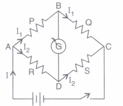
Junction rule: At any junction; the sum of the currents entering the junction is equal to the sum of currents leaving the junction.
Alternatively, Δ i = 0
Justification: Conservation of charge
Loop rule: The Algebraic sum of charges in the potential around any closed loop involving resistors and cells in the loop is zero.
Alternatively: Δ V = 0, where Δ V is the change in potential
Justification: Conservation of energy
2.
Let the resistivity of the material be \(\rho \).
∴ Resistance of wire,\(\ R=\rho \frac { l }{ A } \)
or \(\rho =\frac { RA }{ l } \)
= \(\quad \frac { 5\times 6\times { 10 }^{ -7 } }{ 15 } \)
= \(2\times { 10 }^{ -7 }\Omega -m\)
Thus the resistivity of the material at the temperature of the experiment is \(2\times { 10 }^{ -7 }\Omega -m\)
3.
Let l be the length of four segments will be l, 2l, 4l, 8l. Their corresponding resistance will be R, 2R, 4R and 8R. Given R = \(2 \ \Omega\)
Resistance of the original wire
= R + 2 R + 4 R + 8 R
= 15 R
= 15 x 2
= 30Ω
4.
In a pure semiconductors (Ge or Si) called intrinsic semiconductor the electrically conductivity is related by the electrons thermally excited from the valence band to the conduction band. There are equal number densities of free electrons and holes in conduction band and valence band of intrinsic semiconductor.
When a pure semiconductor of Ge or Si is doped with impurity atoms of valence three (like B or A1), some additional energy levels are created just above the upper energy level of valence band. Due to it, band gap of \(p\)-type semiconductor becomes smaller than intrinsic semiconductor. Also in \(p\)-type semiconductor, the number density of holes is more than that of electrons.
A \(p\)-type semiconductor is obtained when a trivalent atoms (Bor A1) are doped in pure semiconductor of Ge or Si. Here each doped trivalent atom shares its three valence electrons with the three atoms of Ge or Si and form bonds. While the fourth bond remains unbounded. Due to it, a hole is created. Since the impurity atoms and atoms of semiconductor are electrically neutral, hence \(p\)-type semiconductor is also neutral.
5.
Note that thermally generated electrons (ni ~1016m–3) are negligibly small as compared to those produced by doping.
Therefore, ne \(\approx\) ND
Since ne nh = \(n_{i}^{2}\) , The number of holes
nh = (2.25 x 1032 ) / (5 x10²²)
= ~ 4.5 x 10⁹ m–3
6.
1.2\(\Omega\)
7.
As we know E = V + Ir and \(V=\frac{E}{2}, r=1 \Omega\)
\(\therefore E=\frac{E}{2}+I r \ \Rightarrow \ I=\frac{E}{2 r}=\frac{1.5}{2 \times 1}=0.75 \mathrm{~A}\)
8.
The circuit diagram of a full-wave rectifier.
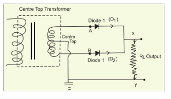
The working principle of full rectifier ;
The full-wave rectifier converts alternating input to variable DC output. It uses the principle of operation of the diode in forward and reverse bias condition. During the positive half cycle of the AC input wave, D1 is forward bias and D2 is reverse bias. We get a positive output at the voltage. During the negative half cycle of the AC input wave, D2 is forward bias and D1 is reverse bias. We get a positive output at the voltage.
9.
The donor energy level ED is just below the bottom of the conduction band. At room temperature this small energy gap is easily converted by the thermally excited electrons. The conduction band has more electrons as they have been contributed both by thermal excitation and donor impurities. Whereas the acceptor energy level EA lies slightly above the top of the valence band. At room temperature, many electrons of the valence band get excited to these acceptor energy levels, leaving behind equal number of holes in the valence band. These holes can conduct current. Thus, the valence band has more holes than the electrons in the conduction band.
10.
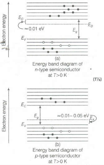
In n-type extrinsic semiconductors, the number of free electrons in conduction band is much more than the number of holes in valence band. The donor energy level lies just below the conduction band. In p-type extrinsic semiconductor, the number of the holes in valence band is much more than the number of free electrons in conduction band. The acceptor energy level lies just above the valence band.
(ii) .png)
At absolute zero temperature (0 K) conduction band of semiconductor is completely empty, i.e., σ=0
Hence, the semiconductor behaves as an insulator. At room temperature, some valence electrons acquire enough thermal energy and jump to the conduction band where they are free to conduct electricity. Thus, the semiconductor acquires a small conductivity at room temperature.
11.
No current flows through 4Ω resistor as capacitor offers infinite resistance in DC circuits.
Also, 2Ω and 3Ω are in parallel combination
∴ RAB = \(\frac { 2\times 3 }{ 2+3 } =\frac { 6 }{ 5 } \)
Applying Kirchhoffs second rule in outer loop AB and cell.
Let I current flow through outer loop in clockwise direction.
-1.2I - 2.8I + 6 = 0
4I = 6
I = 3/2A
∴ Potential difference across AB
VAB = IRAB = 3/2 x 1.2 = 1.8V
∴ 3Ω and 2Ω are in parallel combination.
∴ Potential difference across 2Ω resistor is given by
I = \(\frac { V }{ R } =\frac { 1.8 }{ 2 } \) = 0.9A
I = 0.9 A
12.
Drift velocity: The average velocity with which the free electrons drift under the influence of an external field.
Relaxation time: Average time interval between two successive collisions of an electron with the ions/atoms of the conductor.
The drifts velocity will be inversely proportional to (or \(v_b\ \propto \frac{1}{l}\) ) and hence it will become one-third of 1 its initial value.
13.
Let n electrons pass through wire in 2 minutes, when a current of 300 mA or 0.3A pass for 2 minutes
Charge passing = I = dt =
\(0.3\times 120=36\quad C\)
\(Also \ charge \ with \ n \ electrons\)
\( =n\times 1.6\times { 10 }^{ -19 }C\\ n\times 1.6\times { 10 }^{ -19 }=36\)
\(\\ or\quad n=\frac { 36 }{ 1.6\times { 10 }^{ -19 } } \)
\(\\ =\frac { 360 }{ 16 } \times { 10 }^{ 19 }\)
\(\\ n=22.5\times { 10 }^{ 19 }\)
14.
Given
\({ R }_{ 1 }=1\Omega ,{ R }_{ 2 }=2\Omega ,{ R }_{ 3 }=3\Omega \)
(a) Total resistance of series combination
\({ R }_{ s }={ R }_{ 1 }+{ R }_{ 2 }+{ R }_{ 3 }\)
\({ R }_{ s }\) = 1 + 2 + 3 = \(6\Omega \)
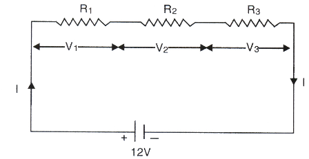
(b) Since E = I (R + r)
I = \(\frac { E }{ { R }_{ s }+0 } =\frac { E }{ { R }_{ s } } =2A\)
\({ V }_{ 1 }={ IR }_{ 1 }=2\times 1=2V\)
\({ V }_{ 2 }={ IR }_{ 2 }=2\times 2=4V\)
\({ V }_{ 3 }={ IR }_{ 3 }=2\times 3=6V\)
15.
Given, input frequency = 50 Hz
For a half-wave rectifier, the output frequency is equal to the input frequency.
\(\therefore\) Output frequency=50 Hz
For a full wave rectifier, the output frequency is twice the input frequency
\(\therefore\) Output frequency = 2 \(\times\) 50 = 100 Hz.
16.
(a) In case of an intrinsic semiconductor the number density of free electrons is equal to number density of holes. There are no external impurity atoms in the intrinsic semiconductors and the conductivity is low in comparison to that of doped (extrinsic semiconductors). When the intrinsic semiconductor is doped with acceptor impurity atoms, a p-type semiconductor is formed. In case of p-type semiconductor, nh >> ne. Therefore, the conductivity of p-type semiconductor is higher than that of the intrinsic semiconductor.
The number of negatively charged immobile ions is equal to the number of oppositively charged holes. Therefore, p type semi-conductor is electrically neutral.
(b) The heavy doping of p and n sides of a p-njunction results into a reduced width of depletion region. As, for the same value of barrier potential, the width decreases and the electric field across the junction Increases.
\(\text { i.e. } \ V=E d \Rightarrow E=\frac{V}{d}\)
As, the electric field of the junction acquires very high value for a large variation of current, the potential difference in breakdown region remains almost same.
This property of zener diode is used in voltage regulation. Zener diode as a voltage regulator.
The unregulated de is given as an input through a series resistor Rs . The zener is always kept under reverse bias. As the input voltage increases, the current through resistance Rs and zener increases. This causes more voltage rise in resistance Rs keeping the voltage across Z the same. This is possible, as at zener voltage, the current increases without any change in potential. As the input drops, the current through resistance Rs and Z drops causing no change in voltage across zener. Thus, at both higher and lower potential inputs, a regulated output is obtained.
17.
It states that current flowing through a conductor is proportional to the potential difference across its two ends provided the physical conditions of the conductor remain unchanged.
If V is the potential difference between two ends of a conductor and I is the current flowing through it, then
\(V\alpha I\)
\(V=RI\)
Where R is the constant of proportionality and is called the resistance of the conductor. Its value depends upon
(i) Shape of the conductor
(ii) Length of conductor
(iii) Nature of the material
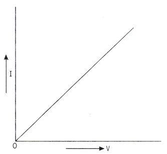
If a graph is plotted between V and I, the graph will be a straight line passing through the origin.
(b) Resistance is the property of a material by virtue of which it opposes the flow of current through it and quantitatively it is given by,
\(R=\frac { V }{ I }\)
\( =\frac { Potential \ difference }{ Current } \)
definition of ohm
Hence a conductor has a resistance of one ohm if a current of one ampere flows through it when a potential difference of one volt is maintained across its two ends.
18.
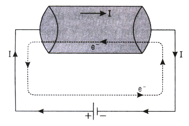
(a) Electric current: The flow of charge in a definite direction constitutes the electric current and the rate of flow of charge through any cross-section of a conductor is the measure of current i.e.,
\(=\frac { Total \ charge \ flowing \ (q) }{ Time \ taken \ (t) } \)
If dq charge is flowing through a section of a conductor in time dt, the electric current is given by
\(I=\frac { dq }{ dt } \)
Unit of electric current S.I unit of current is ampere. It is also called the practical unit of current. It is denoted by A,
\(1 \ ampere(A)=\frac { 1 \ coulomb }{ 1 \ second } = \ 1C{ s }^{ -1 }\)
Thus the current through a wire is said to be 1 ampere if one coulomb of charge is flowing per second through a section of the wire.
Current is a scalar quantity, the direction of flow of positive charges is considered as a conventional direction of the current.
In solids, positive charges being heavy do not move and currently is due to free electrons, therefore, the conventional direction of current is opposite to electronic current.
\(I=\frac { q }{ t } =\frac { ne }{ t } \)
\(n=\frac { It }{ e } =\frac { 1\times 1 }{ 1.6\times { 10 }^{ -19 } } \)
\(=6.25\times { 10 }^{ 18 }electrons \ per \ second.\)
19.
(b)
R < r
20.
(b)
\({2\over 3}Ω\)
21.
(d)
none of the above characteristics
22.
(a)
2R/3
23.
(d)
n2Rp
24.
(a)
vd/4
25.
26.
(d)
decreases exponentially
27.
(b)
\((E_{ g })_{ C, }>({ E }_{ g })_{ si }>\ { (E }_{ g })_{ Ge }\)
28.
(d)
all of the above
29.
(a)
germanium is doped with arsenic
30.
(d)
metallic
31.
(i) (c) :In insulator, energy band gap is > 3 eV
(ii) (b) : In conductor, separation between conduction and valence bands is zero and in insulator, it is greater than 1 eV. Hence in semiconductor the separation between conduction and valence band is 1 eV.
(iii) (a): According to band theory the forbidden gap in conductors Eg = 0, in insulators Eg > 3 eV and in semiconductors Eg < 3 eV.
(iv) (a): The four valence electrons of C, Si and Ge lie respectively in the second, third and fourth orbit.Hence energy required to take out an electron from these atoms (i.e. ionisation energy Eg) will be least for Ge, followed by Si and highest for C. Hence, the number of free electrons for conduction in Ge and Si are significant but negligibly small for C.
(v) (b)
32.
(I) (b): \(q=10^{6} \times 1.6 \times 10^{-19} \mathrm{C}=1.6 \times 10^{-13} \mathrm{C}\)
t = 10-3 s
\(I=\frac{q}{t}=\frac{1.6 \times 10^{-13}}{10^{-3}}=1.6 \times 10^{-10} \mathrm{~A}\)
(ii) (C): C S-1
(iii) (C): The current flowing through a conductor of non-uniform cross-section remain same in the whole of the conductor.
(iv) (a): When a constant current is flowing through a conductor of non-uniform cross-section, electron density does not depend upon the area of cross section, while current density, drift velocity and electric field all vary inversely with area of cross-section.
(v) (a): Given, I = 40 A ;A = 10m2
\(\therefore\) Current density, \(J=\frac{I}{A} \text { or } J=\frac{40}{10}=4 \mathrm{~A} / \mathrm{m}^{2}\)
33.
(c): In a semiconductor, there are no free electrons at 0 K. The number of free electrons increases with increase in temperature because with increase in temperature the electron get sufficient energy to cross forbidden band and reach conduction band. But total number of free electrons in a semiconductor is less than that in a conductor.
34.
(c): Due to diffusion of holes from the p-region to the n-region and of electrons from the n-region to the p-region an electric field is set up across the junction barrier. Once the depletion layer is formed it is in equilibrium and becomes free of mobile charge carriers.
35.
(b): On increasing temperature of wire the kinetic energy of free electrons increase and so they collide more rapidly with each other and hence their drift velocity decreases. Also when temperature increases, resistance increase and resistance is inversely proportional to conductivity of material.
36.
(b): Current is a scalar quantity, it is justified by the following two observations
(i) If current carrying wire is bent at some point, then also current in the wire remains same, while a vector quantity always changes by changing its direction.
(ii) Current flowing in the circuit do not follow the laws of vector addition. It follows according to ordinary rule of algebra. This makes it clear that current is not a vector but a scalar quantity. Also current is defined as rate of flow of charge through the wire 1= dq/ dt.

12th Standard CBSE Syllabus & Materials
12th Standard CBSE
CBSE 12th Computer Science Python Revision Tour I - New Previous year Question Papers Study Material - QB365 Set A
NEW12th Standard CBSE
CBSE 12th Business Studies Planning Important Questions And Answers Study Material - QB365 Set A
NEW12th Standard CBSE
CBSE 12th Business Studies Business Environment Important Questions And Answers Study Material - QB365 Set A
NEW12th Standard CBSE
CBSE 12th Business Studies Principles of Management Important Questions And Answers Study Material - QB365 Set A



NCERT Books

Syllabus

Exam Pattern

Sample Question Papers

Previous year Question Papers

Important Notes

MCQ Practice test

NCERT Exemplers

Case study Questions

Image Based Questions

Passage based Questions

HOT Questions

Value Based Questions

Model Questions Papers
NCERT ( Book Back ) Questions

Assertion and Reason
Important Questions And Answers

CBSE 12th Standard CBSE Subjects
CBSE Standards