100% FREE ACCESS
12th Standard CBSE Syllabus & Materials
12th Standard CBSE
CBSE 12th Economics Government Budget and the Economy Previous year Question Papers Study Material - QB365 Set A
NEW12th Standard CBSE
CBSE 12th Computer Science Interface Python with MySQL - New Previous year Question Papers Study Material - QB365 Set A
NEW12th Standard CBSE
CBSE 12th Computer Science Database Concept - New Previous year Question Papers Study Material - QB365 Set A
NEW12th Standard CBSE
CBSE 12th Computer Science Data Communication - New Previous year Question Papers Study Material - QB365 Set A
NEW12th Standard CBSE
CBSE 12th Computer Science Data Structures - New Previous year Question Papers Study Material - QB365 Set A
NEW12th Standard CBSE
CBSE 12th Computer Science Functions - New Previous year Question Papers Study Material - QB365 Set A

Published on: 23/09/2019
Electronic Devices
Download CBSE Class 12th Standard CBSE Physics question papers, sample papers, important questions, and previous year solved papers in PDF format. Get free study materials, NCERT solutions, and exam preparation resources for Class 12th Standard CBSE Physics
Questions + Answers key
Take MCQ Physics Test
1.
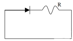
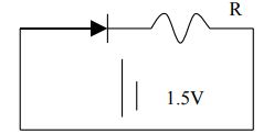
The diode shown in the figure has a constant voltage drop of 0.5V at all currents and a maximum power rating of 100mW. What should be the value of resistance R connected in series, for maximum current.?
2.
Three photo diodes D1 , D2 and D3 are made of semiconductor having band gaps of 2.5 eV, 2eV and 3 eV respectively. Which one will be able to detect light of wavelength 600 \(\overset{o}{A}\)?
3.
Give reason for the following:
(i) High reverse voltage do not appear across a LED.
(ii) Sunlight is not always required for the working of a solar cell.
(iii) The electric field, of the junction of a Zener diode, is very high even for a small reverse bias voltage of about 5 V.
4.
(i) Describe the working principle of a solar cell Mention three basic processes involved in the generation of emf.
(ii) Why are Si and GaAs preferred materials for solar cells.
5.
Write the two processes that take place in the formation of a p-n. junction. Explain with the help of a diagram, the formation of depletion region and barrier potential in a p-n. junction.
6.
On doping germanium with donor atoms of density \({ 10 }^{ 17 }\ cm^{ -3 }\), find its conductivity if mobility of electrons is \(3800\ cm^{ 2 }/V-s\) and intrinsic carrier concentration is \(2.5\times 10^{ 13 }\ cm^{ -3 }\) . Also, find the ratio of conductivity of doped germanium and pure germanium.
7.
A p-type semiconductor has acceptor energy level 53 meV above the valence band. Find the maximum wavelength of light that can create a hole. Use \(h=6.63\times 10^{ -34 }Js, \ c=3\times 10^{ 8 } \ ms^{ -1 }\)
8.
In the circuit \({ V }_{ s }=0.2\ V,{ V }_{ 0 }=-10V\). Find \({ V }_{ e }\), Gain \({ A }_{ u }=\frac { { V }_{ 0 } }{ V_{ c } } \) and \({ A }_{ 0 }=\frac { { V }_{ 0 } }{ V_{ s } } \)
9.
To reduce the ripples in a rectifier circuit with capacitor filter
(a) \(R_{ L }\) should be increased
(b) input frequency should be decreased.
(c) input frequency should be increased.
(d) Capacitors with high capacitance should be used.
10.
When an electronic field is applied across a semiconductor
(a) electrons move from lower energy level to lower energy level in the conduction band.
(b) electrons move from higher energy level to lower energy level in the conduction band.
(c) holes in the valence band move from higher energy level to lower energy level.
(d) holes in the valence band move from lower energy level to higher energy level
11.
Two amplifiers are connected one after the other in series (cascaded). The first amplifier has a voltage gain of 10 and the second has a voltage gain 20. If the input signal is 0.01 volt, Calculate the output ac signal.
1.
e.m.f of the source , E = 1.5
Voltage drop across the diode , Vd = 0.5 V
Maximum power rating of the diode
I = (P / Vd)
I = 0.2A
Potential drop across resistance R
V = E - Vd
= 1 V
R = V/1 = 1/0.2 = 5 \(\Omega \)
2.
Given, wavelength of light,
A = 6000\(\overset{o}{A}\) = 6000 x 10-10 m
\(\therefore\) Energy of the light photon,
\(E=\frac{h c}{\lambda}=\frac{6.6 \times 10^{-34} \times 3 \times 10^{8}}{6000 \times 10^{-10} \times 1.6 \times 10^{-19}} \mathrm{eV}=2.06 \mathrm{eV}\)
The incident radiation which is detected by the photodiode having energy should be greater than the band gap. So, it is only valid for diode D2 . Then, diode D2 will detect this radiation.
3.
(i) It is because reverse break down voltage of LED is very low i.e., nearly 5 V.
(ii) Because solar cell can work with any light whose photon energy is more than the band gap energy.
(ill) The heavy doping of p and n sides of p-n junction, makes the deplection region very thin, hence for a small reverse bias voltage, electric field is very high.
4.
Principle A solar cell works on the principle of photo voltaic effect according to which when light photons of energy greater than energy band gap of a semiconductor are incident on p-n junction of that semiconductor, electron-hole pairs are generated which give rise to an emf. Thus, working principle of a solar cell is same as that of a photodiode. However, no bias is applied in a solar cell and the junction area is kept much larger so that more solar radiation may be incident.
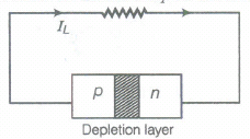
Generation of emf: Three basic processes are involved in the generation of emf by a solar cell when solar radiations are incident on it. These are
(a) the generation of electron-hole pairs close to the junction due to incidence of light with photo energy hv ≥ b.
(b) the separation of electrons and holes due to the electric field of the depletion region. So, electrons are swept to n-side and holes to p-side.
(c) the electrons reaching the 11-side are collected by the front contact and holes reaching p -side are collected by the back contact. Thus, p-side becomes positive and n-side become negative giving rise 1Q a photovoltage. When an external load RL is connected as shown in figure, a photocurrent IL begins to flow through the load.
5.
Two processes that takes place during the formation of p-n junction are diffusion and drift of charge carriers. In an n-type semiconductor, the concentration of electrons is more than that of holes. Similarly, in a p-type semiconductor, the concentration of holes is more than that of electrons. Formation of depletion region during formation of p-n junction and due to the concentration gradient across p and n-sides, holes diffuse from p-side to n-side
(p ⟶ n) and electrons diffuse from n-side to p-side (n ⟶ p). The diffused charge carriers combine with their counterparts in the immediate vicinity of the junction and neutralise.
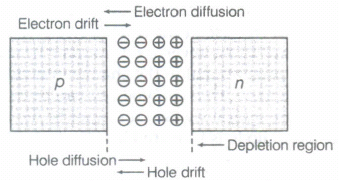
This sets up potential difference across the junction and an internal electric field E; directed from n-side to p-side. The equilibrium is established when the field E; becomes strong enough to stop further diffusion of the majority charge carriers (however, it helps the minority charge carriers to drift across the junction). The region on either side of the junction which becomes depleted (free) from the mobile charge carriers is called depletion region or depletion layer. The potential difference developed across the depletion region is called the potential barrier.
6.
\(\sigma = \ n_{ e } \ \mu _{ e }=10^{ 17 }\times 1.6\times 10^{ -19 }\times 3800\)
\(60.8\ S\ cm^{ -1 }\)
\(\\ \frac { \sigma _{ d } }{ \sigma _{ i } } =\frac { n_{ d } }{ n_{ i } } =\frac { 10^{ 17 } }{ 2.5\times 10^{ 13 } } =4\times 10^{ 3 }:1\)
7.
Here, \(E=53meV=53\times 10^{ -3 } \ eV\)
\(=53\times 10^{ -3 }\times 1.6\times 10^{ -19 }J\)
\(=53\times 1.6\times 10^{ -22 }J\)
Max. Wavelength, \(\lambda _{ max }=\frac { hc }{ E } \)
\(=\frac { \left( 6.63\times 10^{ -34 } \right) \times (3\times 10^{ 8 }) }{ 53\times 1.6\times 10^{ -22 } } =2.35\times 10^{ -5 }m\)
8.
\({ V }_{ c }={ V }_{ s }+{ V }_{ F }={ V }_{ s }+\frac { { V }_{ 0 } }{ 100 } \)
or
\({ V }_{ c }=0.2+\frac { -10 }{ 100 } \)
\(=0.2-0.1=0.1\)
\({ A }_{ 0 }=\frac { { V }_{ 0 } }{ { V }_{ c } } =\frac { -10 }{ 0.1 } =\frac { -10 }{ 0.1 } =-100\)
\({ A }_{ 0 }=\frac { -10 }{ 0.2 } =-50\)
9.
(a), (b), (d)
Since ripple factor with capacitor filter is:
\(\gamma =\frac { 1 }{ \sqrt [ 4 ]{ 3R_{ L } } { C }v } ,\)
So \(\gamma \propto \frac { 1 }{ R_{ L } } ,\ \gamma \propto \frac { 1 }{ C } ,\gamma \propto \frac { 1 }{ v } \)
So to reduce \(\gamma \) , Increase \(R_{ L }\) , C and V.
10.
(a), (c) Knowledge based question
11.
Voltage gain of the first amplifier, V1 = 10
Voltage gain of the second amplifier, V2 = 20
Input signal voltage, Vi = 0.01 V
Output AC signal voltage = Vo
The total voltage gain of a two-stage cascaded amplifier is given by the product of voltage gains of both the stages, i.e.,
V = V1 x V2
= 10 x 20 = 200
We have the relation:
\(V=\frac{V_{0}}{V_{1}}\)
V0 = V x Vi
= 200 x 0.01 = 2 V
Therefore, the output AC signal of the given amplifier is 2 V.

12th Standard CBSE Syllabus & Materials
12th Standard CBSE
CBSE 12th Computer Science Python Revision Tour I - New Previous year Question Papers Study Material - QB365 Set A
NEW12th Standard CBSE
CBSE 12th Business Studies Planning Important Questions And Answers Study Material - QB365 Set A
NEW12th Standard CBSE
CBSE 12th Business Studies Business Environment Important Questions And Answers Study Material - QB365 Set A
NEW12th Standard CBSE
CBSE 12th Business Studies Principles of Management Important Questions And Answers Study Material - QB365 Set A



CBSE 12th Standard CBSE Subjects
CBSE Standards