100% FREE ACCESS
12th Standard CBSE Syllabus & Materials
12th Standard CBSE
CBSE 12th Economics Government Budget and the Economy Previous year Question Papers Study Material - QB365 Set A
NEW12th Standard CBSE
CBSE 12th Computer Science Interface Python with MySQL - New Previous year Question Papers Study Material - QB365 Set A
NEW12th Standard CBSE
CBSE 12th Computer Science Database Concept - New Previous year Question Papers Study Material - QB365 Set A
NEW12th Standard CBSE
CBSE 12th Computer Science Data Communication - New Previous year Question Papers Study Material - QB365 Set A
NEW12th Standard CBSE
CBSE 12th Computer Science Data Structures - New Previous year Question Papers Study Material - QB365 Set A
NEW12th Standard CBSE
CBSE 12th Computer Science Functions - New Previous year Question Papers Study Material - QB365 Set A

Published on: 16/09/2019
Electronic Devices
Download CBSE Class 12th Standard CBSE Physics question papers, sample papers, important questions, and previous year solved papers in PDF format. Get free study materials, NCERT solutions, and exam preparation resources for Class 12th Standard CBSE Physics
Questions + Answers key
Take MCQ Physics Test
1.
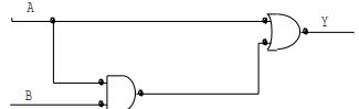
Express by a truth table the output Y for all possible inputs A and B in the circuit shown below
2.
For faster action which transistor is used and why?
3.
How can you relate drift velocity and mobility of an electron?
4.
Write the main use of the
(i) photodiode
(ii) Zener diode.
5.
Distinguish between 'intrinsic' and 'extrinsic' semiconductors?
6.
Name the semiconductor device that can be used to regulate an unregulated de power supply. With the help of I-V characteristics of this device, explain its working principle.
7.
Two car generates have a common gate which needs to open automatically when a car enters either of the garages or cars enter both. A circuit, that resembles this situation using diodes for this situation.
8.
There are two semiconductor materials A and B which are made by doping germanium crystal with indium and arsenic respectively. As shown in the figure, the junction of two is biased with a battery. Will the junction be forward bias and reverse bias?

9.
Write the truth for the circuit shown in figure below. Name the gate that the circuit resembles.

10.
Why does the width of depletion layer of a \(p-n\) junction increase in reverse biasing?
11.
How does the conductivity and resistivity change with rise of temperature in case of intrinsic semiconductors?
12.
The energy gap of silicon is 1.14 eV. Find the maximum wavelength at which silicon starts energy absorption.
1.
The output of the AND gate is Y = A.B consequently the input of the OR gate are A and A.B . Then the final Y = A + A.B
| A | B | Y =A.B | A | Y | Y = A +Y |
|---|---|---|---|---|---|
| 0 | 0 | 0 | 0 | 0 | 0 |
| 0 | 1 | 0 | 0 | 0 | 0 |
| 1 | 0 | 0 | 1 | 0 | 1 |
| 1 | 1 | 1 | 1 | 1 | |
2.
For faster action NPN Transistor is used. In an NPN transistor, current conduction is mainly by free electron, whereas in PNP type transistor. It is mainly holes Since electron are more mobile than holes we prefer NPN for faster action as well as high conduction current.
3.
Mobility of an electron is defined as the drift velocity of electron per unit electric field
i.e \({ \mu }_{ e }={ V }_{ e }/E\)
Mobility of a hole is defined as the drift velocity of hole per unit electric field,
i.e, \({ \mu }_{ h }={ V }_{ h/E }\)
The electrical conductivity \(\sigma \) =1.p =e \(\left( { n }_{ e }{ \mu }_{ e }+{ \mu }_{ h }{ \mu }_{ h } \right) \) where ne & nh are free electron density & hole density respectively
4.
(i) Main use of photodiode In demodulation optical signal and detection of optical signal. In light operated switches, electronic counters.
(ii) Main use of Zener diode As DC voltage regulator.
5.
| Intrinsic semiconductor | Extrinsic semiconductor |
| 1. It is a pure semiconductor material with no impurity atoms in it. | It is prepared by doping a small quantity of impurity atoms to the pure semiconductor. |
| 2. The number of free electrons in the conduction band and the number of holes in valence band is exactly equal. ne = nh = ni |
The number of free electrons and holes is never equal. There is an excess of electrons in n-type ne > ni semiconductors and excess of holes in p-type nh > ni semiconductors. |
6.
Zener diode
Alternatively
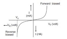
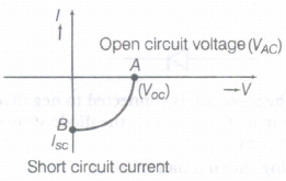
After the breakdown voltage, there is an insignificant change in the (reverse) bias voltage across the Zener diode (and hence the load) even for large changes in current.
7.
As, car enters in the gate, any one or both are opened. The device is shown below:

So, OR gate gives the desired output
| A | B | C |
| 0 | 0 | 0 |
| 0 | 1 | 1 |
| 1 | 0 | 1 |
| 1 | 1 | 1 |
8.
As, semiconductor A is doped with indium, so it behaves as p-type semiconductor and B is doped with arsenic so, it behaves as n-type semiconductor. Thus, the figure shows that it is forward bias condition.
9.
The circuit resembles AND gate. The BOOLEAN expression of this circuit is, V0 = A.B i.e. V0 equals A AND B. The truth table of this gate is as given below:
| A | B | V0 = A.B |
| 0 | 0 | 0 |
| 0 | 1 | 0 |
| 1 | 0 | 0 |
| 1 | 1 | 1 |
10.
When \(p-n\) junction is reversed biased, the positive terminal of the external battery is connected to \(n-\)-side of \(p-n\) junction and its negative terminal to \(p\)-side of \(p-n\) junction. The positive terminal of the external battery attracts the majority carrier electrons from the \(n\)-region and its negative terminal attracts the majority carrier holes from \(p\)-region. Due to it, the majority charge carriers move away from the junction. This increases the width of the depletion layer.
11.
When the temperature of the semiconductor is raised, more covalent bonds are broken in the given semiconductor. Due to it, there is a large increase in the charge carrier concentration in semiconductor. The fraction \((f)\) of the number of electrons raised from valence band to conduction band at temperature TK in intrinsic semiconductor is given by
\(f\propto e^{ -E_{ g }/2kT }\)
where \(E_{ g }\) is the value of forbidden energy gap. If means, if T increases, \(f\) also increases, i.e., with the increase in temperature, the number of electrons in conduction band increases. This leads to increase in conductivity of intrinsic semiconductor. As resistivity of pure semiconductor decreases with increase in temperature.
12.
Here,\(E=1.14 \ eV=1.14\times 1.6\times 10^{ -19 } \ J\)
\(\\ \lambda =\frac { hc }{ E } =\frac { 6.62\times 10^{ -34 }\times 3\times 10^{ 8 } }{ 1.6\times 10^{ -19 }\times 1.14 } =10,888 \ A°\)

12th Standard CBSE Syllabus & Materials
12th Standard CBSE
CBSE 12th Computer Science Python Revision Tour I - New Previous year Question Papers Study Material - QB365 Set A
NEW12th Standard CBSE
CBSE 12th Business Studies Planning Important Questions And Answers Study Material - QB365 Set A
NEW12th Standard CBSE
CBSE 12th Business Studies Business Environment Important Questions And Answers Study Material - QB365 Set A
NEW12th Standard CBSE
CBSE 12th Business Studies Principles of Management Important Questions And Answers Study Material - QB365 Set A



CBSE 12th Standard CBSE Subjects
CBSE Standards