100% FREE ACCESS
12th Standard CBSE Syllabus & Materials
12th Standard CBSE
CBSE 12th Economics Government Budget and the Economy Previous year Question Papers Study Material - QB365 Set A
NEW12th Standard CBSE
CBSE 12th Computer Science Interface Python with MySQL - New Previous year Question Papers Study Material - QB365 Set A
NEW12th Standard CBSE
CBSE 12th Computer Science Database Concept - New Previous year Question Papers Study Material - QB365 Set A
NEW12th Standard CBSE
CBSE 12th Computer Science Data Communication - New Previous year Question Papers Study Material - QB365 Set A
NEW12th Standard CBSE
CBSE 12th Computer Science Data Structures - New Previous year Question Papers Study Material - QB365 Set A
NEW12th Standard CBSE
CBSE 12th Computer Science Functions - New Previous year Question Papers Study Material - QB365 Set A

Published on: 02/11/2025
Download CBSE Class 12th Standard CBSE Physics question papers, sample papers, important questions, and previous year solved papers in PDF format. Get free study materials, NCERT solutions, and exam preparation resources for Class 12th Standard CBSE Physics
Questions + Answers key
Take MCQ Physics Test
1.
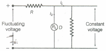
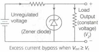
Name the device, D which is used as a voltage regulator in the given circuit and give its symbol.
2.
Carbon and silicon both have four valence electrons each, then how are they distinguished?
3.
When a forward bias applied to a p-n junction, it
(a) raises the potential barrier
(b) reduces the majority carrier current to zero
(c) lowers the potential barrier
(d) None of the above
4.
(i) How is a photodiode fabricated?
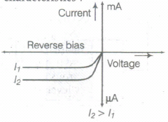
(ii) Briefly explain its working. Draw its V-I characteristics for two different intensities of illumination.
5.
Draw the energy band diagrams of
(i) n-type and
(ii) p-type semiconductor at temperature, T> OK.
In the case n-type Si semiconductor, the donor energy level is slightly below the bottom of conduction band whereas in p-type semiconductor, the acceptor energy level is slightly above the top of the valence band. Explain, what role do these energy levels play in conduction and valence bands.
6.
A Zener diode is fabricated by heavily doping both p- and n- sides of the junction. Explain, why? Briefly explain the use of Zener diode as a DC voltage regulator with the help of a circuit diagram.
7.
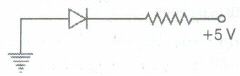
(i) In the following diagram, is the junction diode forward biased or reverse biased?
(ii) Draw the circuit diagram of a full wave rectifier and state how it works?
8.
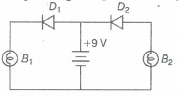
(i) In the following diagram, which bulb out of B1 and B2 will glow and why?
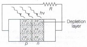
(ii) Draw a diagram of an illuminated p-n. junction solar cell.
(iii) Explain briefly the three processes due to which generation of emf takes place in a solar cell.
9.
Distinguish between a conductor, a semiconductor and an insulator on the basis of energy band diagrams.
10.
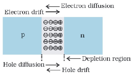
(a) Describe briefly, with the help of a diagram, the role of the two important processes involved in the formation of a p-n junction.
(b) Name the device which is used as a voltage regulator. Draw the necessary circuit diagram and explain its working.
11.
(a) Draw the circuit arrangement for studying the V - I characteristics of a p-n junction diode in (i) forward and (ii) reverse bias. Briefly explain how the typical V - I characteristics of a diode are obtained and draw these characteristics.
(b) With the help of necessary circuit diagram explain the working ot a photo diode used for detecting optical signals.
12.
(a) Explain with the help of a diagram, how a depletion layer and barrier potential are formed in a junction diode
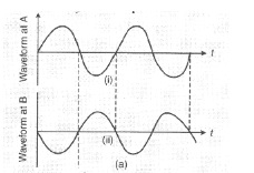
(b) Draw a circuit diagram of full wave rectifier. Explain its working and draw input and output waveforms full wave rectifier. Explain its working and draw input and output waveforms
1.
Device, D is a Zener diode.
Symbol of Zener diode

2.
The four valence electrons of carbon are present in second orbit while that of silicon in third orbit. So, energy required to extricate an electron from silicon is much smaller than carbon. Therefore, the number of free electrons for conduction in silicon is significant on contrary to the carbon. This makes silicons is conductivity much higher than carbon. This is the main distinguishable property.
3.
The correct statement is (c).
When a forward bias is applied to a p-n junction, it lowers the value of potential barrier. In the case of a forward bias, the potential barrier opposes the applied voltage. Hence, the potential barrier across the junction gets reduced.
4.
(a) A photodiode is fabricated by allowing light to fall on a diode through a transparent window. It is fabricated such that the generation of e-n pairs take place near the depletion region.
5.
The donor energy level ED is just below the bottom of the conduction band. At room temperature this small energy gap is easily converted by the thermally excited electrons. The conduction band has more electrons as they have been contributed both by thermal excitation and donor impurities. Whereas the acceptor energy level EA lies slightly above the top of the valence band. At room temperature, many electrons of the valence band get excited to these acceptor energy levels, leaving behind equal number of holes in the valence band. These holes can conduct current. Thus, the valence band has more holes than the electrons in the conduction band.
6.
In Zener diode, both p and n-side of the function are heavily doped. Heavy doping ensures high junction field and low breakdown voltage.
The circuit diagram of a voltage regulator using a Zener diode is shown in figure. The unregulated DC voltage is connected to the Zener diode through a series resistance Rs in reverse biased. Thus, any charge in the input voltage result is charge voltage drop across Rs without any change in voltage across the Zener diode. Therefore, Zener diode acts as a voltage regulator.
7.
The given diagram shown below
.png)
The circuit above can be redrawn as follows
.png)
As the p-section is connected to negative terminal of the battery, the diode shown is reverse biased.
(ii) During the first half of input cycle, the upper end of the coil is at positive potential and lower end at negative potential. The function diode DI is forward biased and D2 in reverse biased. Current flows in output load in the
direction shown in figure. During the second half of input cycle, D2 is forward biased. In this way, current flows in the load in the single direction as shown in figure.
.png)
8.
(i) D1 diode is forward biased, hence current will flow in B1 bulb and D2 is reverse biased, so there will be no current in B2. Hence, BI will glow.
(ii) The diagram of illuminated p-n junction solar cell is given below
(iii) Processes due to generation of emf takes place in a solar cell are given below
(a) When light photon reach the junction, the excited electrons from the valence band to conduction band creating equal number of holes and electrons.
(b) These electron hole pair move in opposite direction due to junction field. Their movement in opposite direction creates potential difference (photo-voltage).
(c) When load is connected in the external circuit, current starts flowing through it due to photo-voltage.
9.
.png)
(a) metals, (b) insulators and (c) semiconductors
Two distinguishing features:
(i) In conductors, the valence band and conduction band tend to overlap (or nearly overlap) while in insulators they are separated by a large energy gap and in semiconductors they are separated by a smaJ1'ep.ergygap.
(ii) The conduction band, of a conductor, has a large number of electrons available for electrical conduction. However the conduction band of insulators is almost empty while that of the semiconductor has only a (very) small number of such electrons available for electrical conduction.
.png)
10.
The two processes are
(i) Diffusion
(ii) Drift
Diffusion : Holes diffuse from p-side to n-side (p \(\rightarrow \) n) and electrons diffuse from n-side to p-side (n\(\rightarrow \) p)
Drift: The motion of charge carriers, due to the applied electric field \((\vec { E } )\) which results in drifting of holes along E and of electrons opposite to that of electric field \((\vec { E } )\)).
(b) Name of device: Zener Diode
Working:
Any increase I decrease in the input voltage results in an increase I decrease of the voltage drop across R,; without any change in voltage across the Zener diode. Thus Zener diode acts as voltage regulator.
11.
.png)
Reverse biasing
.png)
The VI characteristics are obtained by connecting the battery, to the diode, through a potentiometer (or rheostat). The applied voltage to the diode is changed. The values of current, for different values of voltage, are noted and a graph between V and I is plotted. The V-I characteristics, of a diode, have the form shown here.
.png)
(b) The circuit diagram, for the photodiode, is shown here.
.png)
The photodiode is illuminated by optical signal, whose photon energy is greater than the energy gap of the semiconductor used.
The electric field, at the junction, separates the electrons and holes and thus gives rise to an emf.
When an external load is connected, a (photo) current flows through it. The magnitude of this current is proportional to the intensity of light incident on the photodiode.
12.
.png)
(a) Due to the diffusion of electrons and the holes, from their majority zone to minority zone, a layer of positive and negative space charge region on either side on the junction is formed. This is called the depletion region.
The loss of electrons, from n-region and gain of electrons by the p-region, causes a difference of potential across the junction. This tends to prevent the movement of charge carriers across the junction and is, therefore, termed as barrier potential.
.png)
For positive half cycle of input ac, one of the two diodes gets forward biased and conducts and output current is obtained across the load RL, For negative half cycle of input ac, the other diode
gets forward biased and thus output current is obtained due to it. Therefore, output is obtained for both the cycles of input ac.
.png)

12th Standard CBSE Syllabus & Materials
12th Standard CBSE
CBSE 12th Computer Science Python Revision Tour I - New Previous year Question Papers Study Material - QB365 Set A
NEW12th Standard CBSE
CBSE 12th Business Studies Planning Important Questions And Answers Study Material - QB365 Set A
NEW12th Standard CBSE
CBSE 12th Business Studies Business Environment Important Questions And Answers Study Material - QB365 Set A
NEW12th Standard CBSE
CBSE 12th Business Studies Principles of Management Important Questions And Answers Study Material - QB365 Set A



NCERT Books

Syllabus

Exam Pattern

Sample Question Papers

Previous year Question Papers

Important Notes

MCQ Practice test

NCERT Exemplers

Case study Questions

Image Based Questions

Passage based Questions

HOT Questions

Value Based Questions

Model Questions Papers
NCERT ( Book Back ) Questions

Assertion and Reason
Important Questions And Answers

CBSE 12th Standard CBSE Subjects
CBSE Standards