100% FREE ACCESS
12th Standard CBSE Syllabus & Materials
12th Standard CBSE
CBSE 12th Economics Government Budget and the Economy Previous year Question Papers Study Material - QB365 Set A
NEW12th Standard CBSE
CBSE 12th Computer Science Interface Python with MySQL - New Previous year Question Papers Study Material - QB365 Set A
NEW12th Standard CBSE
CBSE 12th Computer Science Database Concept - New Previous year Question Papers Study Material - QB365 Set A
NEW12th Standard CBSE
CBSE 12th Computer Science Data Communication - New Previous year Question Papers Study Material - QB365 Set A
NEW12th Standard CBSE
CBSE 12th Computer Science Data Structures - New Previous year Question Papers Study Material - QB365 Set A
NEW12th Standard CBSE
CBSE 12th Computer Science Functions - New Previous year Question Papers Study Material - QB365 Set A

Published on: 07/03/2026
Download CBSE Class 12th Standard CBSE Physics question papers, sample papers, important questions, and previous year solved papers in PDF format. Get free study materials, NCERT solutions, and exam preparation resources for Class 12th Standard CBSE Physics
Questions + Answers key
Take MCQ Physics Test
1.
What happens to the width of depletion layer of a p-n junction when it is
(i) forward biased,
(ii) reverse biased?
2.
A student wants to use two p-n junction diodes to convert alternating current into direct current. Draw the labelled circuit diagram she would use and explain how it works.
3.
State the relation for the voltage gain in terms of trans-conductance, using transistor as an amplifier.
4.
What is the direction of diffusion current in a junction diode?
5.
Where does the fermi-level of intrinsic semiconductor lie?
6.
Write the two processes that take place in the formation of a p-n. junction. Explain with the help of a diagram, the formation of depletion region and barrier potential in a p-n. junction.
7.
The applied input a.c. power to a half wave rectifier is 100 watt. The d.c. output power obtained is 40 watt.
(i) What is the rectification efficiency and
(ii) What is the power efficiency?
8.
Out of the ionic,covalent and metallic and van der Waal's solids, which will be widely used to produce a conductor, semiconductor and insulator?
9.
Find the binary (i) addition (ii) subtraction of the following set of numbers ; 101010 and 010101.
10.
Find the equivalent binary number of decimal number \({ \left( 9.25 \right) }_{ 10. }\)
11.
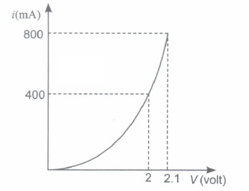
The I-V characteristic of a p-n junction diode is shown below. The approximate dynamic resistance of the p-n junction when a forward bias of 2 volt is applied
1 Ω
0.25 Ω
0.5 Ω
5 Ω
12.
In a common emitter (CE) amplifier having a voltage gain G, the transistor used has transconductance 0.03 mho and current gain 25. If the above transistor is replaced with another one with transconductance 0.02 mho and current gain 20, the voltage gain will be:
\(\frac { 5 }{ 4 } \ G\)
\(\frac { 2 }{ 3 } \ G\)
1.5 G
\(\frac { 1 }{ 3 } \ G\)
13.
In a CE transistor amplifier the audio signal voltage across the collector resistance of \(2k\Omega \)is 2V. If the base resistance is \(1k\Omega \) and the current amplification of the transisitor is 100, the input signal voltage is :
0.1 V
1.0 V
1 mV
10 mV
14.
The barrier potential of a p-n junction depends on :
(i) type of semiconductor material
(ii) amount of doping
(iii) temperature.
Which one of the following is correct?
(i) and (ii) only
(ii) only
(ii) and (iii) only
(i),(ii) and (iii)
15.
A Ge specimen is doped with AI. The concentration of acceptor atoms is \(-10^{ 21 }\) atoms/\(m^{ 3 }\) , the concentration of electrons in the specimen is
\(10^{ 17 }/m^{ 3 }\)
\(10^{ 15 }/m^{ 3 }\)
\(10^{ 4 }/m^{ 3 }\)
\(10^{ 2 }/m^{ 3 }\)
16.
In a npn transisitor circuit,the collector current is 10 mA. If 95 percent of the electrons emitted reach the collector,which of the following statements are true?
The entire current will be 8 mA
The emitter current will be 10.53 mA
The base current will be 2 mA
The base current will be 2 mA
17.
Consider an npn transistor with its base emitter junction forward biased and collector base junction reverse biased. Which of the following statements are true?
Electrons crossover from emitter to collector
Holes move from base to collector
Electrons move from emitter to base
Electrons from emitter move out of base without going to the collector
18.
Hole is
an anti-particle of electron
a vacancy created when an electron leaves a covalent bond
absence of free electron
an artificially created particle
19.
For a transistor action, which of the following statements are correct:
Collector current is equal to the sum of base current and emitter current.
The input resistance depends upon the current \(I_{ c }\) in the transistor
The emitter junction is forward biased and collector junction is reverse biased.
Both the emitter junction as well as the collector junction are reverse biased.
20.
The electrical resistance of depletion layer is large because
it has no charge carriers
it has few holes as charge carriers
it contains few electrons as charge carriers
it contains few ions as charge carriers
21.
From the output characteristics shown in Fig.(b), calculate the values of \(\beta\)ac and \(\beta\)dc of the transistor when VCE is 10 V and I C = 4.0 mA
22.
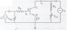
(a) Draw the circuit diagram of an n-p-n transistor with emitter-base junction forward biased and collector-base junction reverse biased. Describe briefly how the motion of charge carriers in the transistor constitutes the emitter current (IE), the base current (IB) and the collector current (IC ). Hence deduce the relation IE = IB + IC.
(b) Explain with the help of a circuit diagram how a transistor works as an amplifier.
23.
(a) Explain with the help of a diagram, how a depletion layer and barrier potential are formed in a junction diode
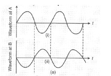
(b) Draw a circuit diagram of full wave rectifier. Explain its working and draw input and output waveforms full wave rectifier. Explain its working and draw input and output waveforms
24.
(i) Differentiate between three segments of a transistor on the basis of their size and level of doping
(ii) How is a transistor biased to be in active state?
(iii) With the help of necessary circuit diagram, describe briefly how n-p-n transistor in CE configuration amplifies a small sinusoidal input voltage. Write the expression for the AC current gain.
25.
\(p-n\) junction is a semiconductor diode.It is obtained by bringing \(p-\) type semiconductor include contact with \(n-\) type semiconductor. A thin layer is developed at the \(p-\) junction which is devoid of any charge carrier but has immobile ions. It is called depletion layer. At the junction a potential barrier appears, which does not allow the movement of majority charge carriers across the junction in the absence of any biasing of the junction.
\(p-\)n junction offers low resistance when forward biased and high resistance when reverse biased. Read the above paragraph and answer the following questions:
(i) Can we measure the potential barrier of \(p-n\) junction by putting a sensitive voltmeter across its terminals?
(ii) What practical lesson do you draw from the above study?
26.
27.
A silicon p-n junction diode is connected to a resistor R and a battery of voltage VB through milliammeter (mA) as shown in figure. The knee voltage for this junction diode is VN = 0.7 V. The p-n junction diode requires a minimum current of 1m. A to attain a value higher than the knee point on the J- V characteristics of this junction diode. Assuming that the voltage V across the junction is independent of the current above the knee point. A p-n junction is the basic building block of many semiconductor devices like diodes. Important process occurring during the formation of a p-n junction are diffusion and drift. In an n-type semiconductor concentration of electrons is more as compared to holes. In a p-type semiconductor concentration of holes is more as compared to electrons.
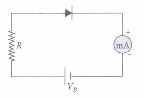
(i) If VB = 5 V, the maximum value of R so that the voltage V is above the knee point voltage is
| (a) 40 \(\Omega\) | (b) 4.3 \(\Omega\) | (c) 5.0 \(\Omega\) | (d) 5.7 \(\Omega\) |
(ii) If VB = 5 V, the value of R in order to establish a current to 6 mA in the circuit is
| (a) 833 \(\Omega\) | (b) 717 \(\Omega\) | (c) 950 \(\Omega\) | (d) 733 \(\Omega\) |
(iii) If VB = 6 V, the power dissipated in the resistor R, when a current of 6 mA flows in the circuit is
| (a) 30.2 mW | (b) 30.8 mW | (c) 31.2 mW | (d) 31.8 mW |
(iv) When the diode is reverse biased with a voltage of 6 V and Vbi = 0.63 V. Calculate the total potential.
| (a) 9.27 V | (b) 6.63 V | (c) 5.27 V | (d) 0.63 V |
(v) Which of the below mentioned statement is false regarding a p-n junction diode?
| (a) Diodes are uncontrolled devices. | (b) Diodes are rectifying devices. |
| (c) Diodes are unidirectional devices. | (d) Diodes have three terminals |
28.
29.
1.
(i) The width of depletion layer decreases.
(ii) The width of depletion layer increases
2.
A rectifier is used to convert alternating current into direct current, whose labelled circuit is given below.
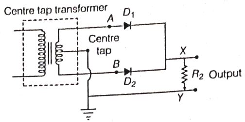
Working
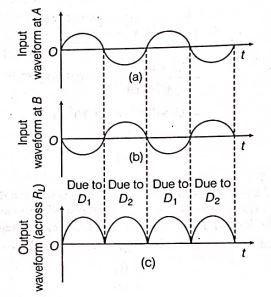
During the positive half cycle of the input AC, the diode D1, is forward biased and the diode D2 is reverse biased. The forward current flows through diode D1.
During the negative half cycle of the input AC, the diode D1 is reverse biased and diode D2 is forward biased. Thus, current flows through diode D2 . Thus, we find that during both the halves, current flows in the same direction.
3.
Voltage gain \(=-trans-conductance\times output\ resistance \)
4.
In junction diode, the direction of diffusion current is from P-region to N-region.
5.
The fermi-level of intrinsic semiconductor lies mid way between its valence and conduction bands i.e., in the middle of forbidden energy gap of intrinsic semi-conductor.
6.
Two processes that takes place during the formation of p-n junction are diffusion and drift of charge carriers. In an n-type semiconductor, the concentration of electrons is more than that of holes. Similarly, in a p-type semiconductor, the concentration of holes is more than that of electrons. Formation of depletion region during formation of p-n junction and due to the concentration gradient across p and n-sides, holes diffuse from p-side to n-side
(p ⟶ n) and electrons diffuse from n-side to p-side (n ⟶ p). The diffused charge carriers combine with their counterparts in the immediate vicinity of the junction and neutralise.
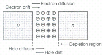
This sets up potential difference across the junction and an internal electric field E; directed from n-side to p-side. The equilibrium is established when the field E; becomes strong enough to stop further diffusion of the majority charge carriers (however, it helps the minority charge carriers to drift across the junction). The region on either side of the junction which becomes depleted (free) from the mobile charge carriers is called depletion region or depletion layer. The potential difference developed across the depletion region is called the potential barrier.
7.
Rectification efficiency
\(=\frac { d.c.output \ power }{ a.c.input \ power } \times100\)
\( =\frac { 40 }{ 100 } \times100=40%\)
Power efficiency
\(=\frac { d.c.output \ power }{ a.c.input \ power \ for \ half \ cycle } \times100\)
\( =\frac { 40 }{ (100/2) } \times100=80%\)
8.
Metallic solids are used to produce good conductors. Covalent solids are generally used to produce semiconductors and the ionic and van der Waal's solids are used to produce insulators.
9.
| (i) | 101010 | (ii) | 101010 |
| +010101 | - 010101 | ||
| _______ | _______ | ||
| 111111 | 010101 | ||
| _______ | _______ |
10.
\({ \left( 9.25 \right) }_{ 10 } \ = \ { \left( 9 \right) }_{ 10 }+{ \left( 0.25 \right) }_{ 10 }\)
\(=\ { \left( 1001 \right) }_{ 2 }+{ \left( 0.01 \right) }_{ 2 }\)
\(=\ { \left( 1001.01 \right) }_{ 2 }\)
11.
(b)
0.25 Ω
12.
13.
(d)
10 mV
14.
(d)
(i),(ii) and (iii)
15.
(a)
\(10^{ 17 }/m^{ 3 }\)
16.
(b)
The emitter current will be 10.53 mA
17.
(c)
Electrons move from emitter to base
18.
(b)
a vacancy created when an electron leaves a covalent bond
19.
(d)
Both the emitter junction as well as the collector junction are reverse biased.
20.
(a)
it has no charge carriers
21.
\(\beta_{a c}=\left(\frac{\Delta I_{C}}{\Delta I_{B}}\right)_{V_{C E}}, \quad \beta_{d c}=\frac{I_{C}}{I_{B}}\)
For determining \(\beta\)ac and \(\beta\)dc at the stated values of VCE and IC one can proceed as follows. Consider any two characteristics for two values of I B which lie above and below the given value of IC. Here IC = 4.0 mA. (Choose characteristics for IB= 30 and 20 \(\mu\)A.) At VCE = 10 V we read the two values of IC from the graph. Then
\(\Delta I_{B}=(30-20) \mu \mathrm{A}=10 \mu \mathrm{A}, \Delta I_{C}=(4.5-3.0) \mathrm{mA}=1.5 \mathrm{~mA}\)
Therefore, \(\beta_{a c}=1.5 \mathrm{~mA} / 10 \mu \mathrm{A}=150\)
For determining \(\beta\)dc, either estimate the value of I B corresponding to I C = 4.0 mA at VCE = 10 V or calculate the two values of \(\beta\)dc for the two characteristics chosen and find their mean.
Therefore, for I C = 4.5 mA and IB = 30 \(\mu\)A
\(\beta_{d c}=4.5 \mathrm{~mA} / 30 \mu \mathrm{A}=150\)
and for IC = 3.0 mA and IB = 20 \(\mu\)A
\(\beta_{d c}=3.0 \mathrm{~mA} / 20 \mu \mathrm{A}=150\)
Hence, \(\beta_{d c}=(150+150) / 2=150\)
22.
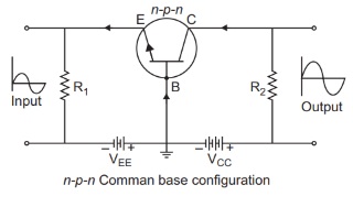
(a) The circuit diagram is shown here:
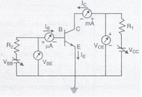
The emitter-base junction, being forward biased, the majority charge carriers (electrons), from the emitter, flow into the base region constituting the emitter current (IE) The base region, being very thin, only a (very) small fraction, of these (small base current (IB). 1 The majority of these charge carriers, are attracted by the (reverse biased) collector. These make up the collector current (IC )
IE = IC + IB
The circuit diagram of a transistor, working as an amplifier, in its C E mode, is shown here.
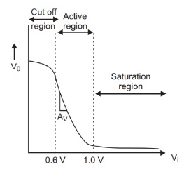
If a small sinusoidal voltage is superimposed on the dc base bias by connecting the source of this signal in series with VBB supply. Then the base current will have sinusoidal variations superposed on the values IB. as a consequence the collector current also will have sinusoidal variation superimposed on the value of IC producing in turn corresponding change in the output voltage V0 .
23.
.png)
(a) Due to the diffusion of electrons and the holes, from their majority zone to minority zone, a layer of positive and negative space charge region on either side on the junction is formed. This is called the depletion region.
The loss of electrons, from n-region and gain of electrons by the p-region, causes a difference of potential across the junction. This tends to prevent the movement of charge carriers across the junction and is, therefore, termed as barrier potential.
.png)
For positive half cycle of input ac, one of the two diodes gets forward biased and conducts and output current is obtained across the load RL, For negative half cycle of input ac, the other diode
gets forward biased and thus output current is obtained due to it. Therefore, output is obtained for both the cycles of input ac.
.png)
24.
(a) Emitter: It is of moderate size and heavily doped
Base: It is very thin and lightly doped Collector : It is moderately doped and larger in size.
(b) Transistor is said to be in active state when its emitter-base junction is (suitably) forward biased and base-collector junction is (suitably) reverse biased.
(c)When a small sinusoidal voltage is superposed on the dc base biased, the base current will have sinusoidal variation superimposed on the value of IE. As a consequence, the collector current also will have sinusoidal variations, superimposed on the
Value of IC, producing corresponding (amplified) changes in the value of V0 .
ac current gain, \({ \beta }_{ ac }={ \left( \frac { \Delta { I }_{ C } }{ \Delta { I }_{ B } } \right) }_{ { V }_{ CB } }\)
25.
(i) We cannot measure the potential barrier of \(p-n\) junction by putting a sensitive voltmeter across its terminals because there are no free electrons or holes in the depletion layer. And in the absence of forward biasing, the depletion layer offers infinite resistance.
(ii) From the above study,we find that when some move supports the tendency of majority of the people, the resistance/(opposition) is lowered and output current (desired result) is large (appreciable) However, when some move is against the tendency of majority of people, it suffers rough weather.
26.
27.
(i) (b) : Voltage drop across R.
\(V_{R}=V_{B}-V_{N}=5-0.7=4.3 \mathrm{~V}\)
Here, Imin = 1 x 10⁻³ A
\(R_{\max }=\frac{V_{R}}{I_{\min }}=\frac{4.3}{1 \times 10^{-3}}=4.3 \times 10^{3} \Omega=4.3 \mathrm{k} \Omega\)
(ii) (b) : \(I=6 \mathrm{~mA}=6 \times 10^{-3} \mathrm{~A}\)
\(\begin{array}{l} V_{R}=V_{B}-V_{N}=5-0.7=4.3 \mathrm{~V} \\ R=\frac{V_{R}}{I}=\frac{4.3}{6 \times 10^{-3}}=717 \Omega \end{array}\)
(iii)(d) : Here, VB = 6 V; VN = 0.7V,
\(V_{R}=6-0.7=5.3 \mathrm{~V}\)
Power dissipated in R = l x VR
= (6 x 10-3) x 5.3 = 31.8 x 10⁻³ W
= 31.8 mW
(iv) (b) : Vt = Vbi + VR = 0.63 + 6 = 6.63 V
(v) (d) : Diode is two terminal device, anode and cathode are the two terminals.
28.
29.

12th Standard CBSE Syllabus & Materials
12th Standard CBSE
CBSE 12th Computer Science Python Revision Tour I - New Previous year Question Papers Study Material - QB365 Set A
NEW12th Standard CBSE
CBSE 12th Business Studies Planning Important Questions And Answers Study Material - QB365 Set A
NEW12th Standard CBSE
CBSE 12th Business Studies Business Environment Important Questions And Answers Study Material - QB365 Set A
NEW12th Standard CBSE
CBSE 12th Business Studies Principles of Management Important Questions And Answers Study Material - QB365 Set A



NCERT Books

Syllabus

Exam Pattern

Sample Question Papers

Previous year Question Papers

Important Notes

MCQ Practice test

NCERT Exemplers

Case study Questions

Image Based Questions

Passage based Questions

HOT Questions

Value Based Questions

Model Questions Papers
NCERT ( Book Back ) Questions

Assertion and Reason
Important Questions And Answers

CBSE 12th Standard CBSE Subjects
CBSE Standards