100% FREE ACCESS
12th Standard CBSE Syllabus & Materials
12th Standard CBSE
CBSE 12th Economics Government Budget and the Economy Previous year Question Papers Study Material - QB365 Set A
NEW12th Standard CBSE
CBSE 12th Computer Science Interface Python with MySQL - New Previous year Question Papers Study Material - QB365 Set A
NEW12th Standard CBSE
CBSE 12th Computer Science Database Concept - New Previous year Question Papers Study Material - QB365 Set A
NEW12th Standard CBSE
CBSE 12th Computer Science Data Communication - New Previous year Question Papers Study Material - QB365 Set A
NEW12th Standard CBSE
CBSE 12th Computer Science Data Structures - New Previous year Question Papers Study Material - QB365 Set A
NEW12th Standard CBSE
CBSE 12th Computer Science Functions - New Previous year Question Papers Study Material - QB365 Set A

Published on: 07/03/2026
Download CBSE Class 12th Standard CBSE Physics question papers, sample papers, important questions, and previous year solved papers in PDF format. Get free study materials, NCERT solutions, and exam preparation resources for Class 12th Standard CBSE Physics
Questions + Answers key
Take MCQ Physics Test
1.
During the formation of a p-n junction
diffusion current keeps increasing
drift current remains constant
both the diffusion current and drift current remain constant.
diffusion current remains almost constant but drift current increases till both currents-become equal
2.
If a p-n junction diode is reverse biased.
the potential barrier is lowered
the potential barrier rermainsunaffected.
the potential barrier is raised
the current is mainly due to majority charge carriers.
3.
The formation of depletion region in a p-n junction diode is due to
movement of dopant atoms
diffusion of the electrons and holes
drift of electrons only
drift of holes only
4.
At a certain temperature in an intrinsic semiconductor, the electrons and holes concentration is 1.5 × 10¹⁶ m-3.When it is doped with a trivalent dopant, hole concentration increases to 4.5 \(\times\) 1022 m-3. In the doped semiconductor, the concentration of electrons (ne) will be
3 x 10⁶ m-3
5 x 10⁷ m-3
5 x 10⁹ m-3
6.75 x 1038 m-3
5.
The I-V characteristic of a p-n junction diode is shown below. The approximate dynamic resistance of the p-n junction when a forward bias of 2 volt is applied
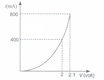
1 Ω
0.25 Ω
0.5 Ω
5 Ω
6.
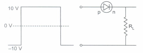
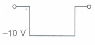
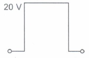
If the following input signal is sent through a p-n junction diode, then the output signal across RL will be
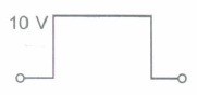
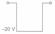
7.
Current in the circuit will be
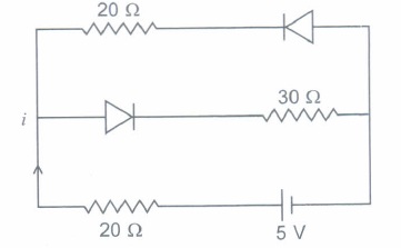
5/40 A
5/50 A
5/10A
5/20 A
8.
A 2V battery is connected across the points A and B as shown in the figure. Assuming that the resistance of each diode is zero in forward bias and infinity in reverse bias, the current supplied by the battery when its positive terminal is connected to A is
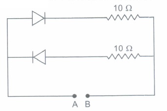
0.2 A
0.4 A
Zero
0.1 A
9.
In a p-type semiconductor, there is
excess of one electron.
absence of one electron
a missing atom.
a donar level
10.
A p-type semiconductor can be obtained by adding
arsenic to pure silicon.
gallium to pure silicon
antimony to pure germanium.
phosphorus to pure germanium
11.
In the circuit shown in figure below, if the diode forward voltage drop is 0.3 V, the voltage difference between A and B is
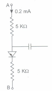
1.3 V
2.3 V
0
0.5 V
12.
A full-wave rectifier circuit along with the input and output voltages is shown in the figure The contribution to output voltage from diode 2 is
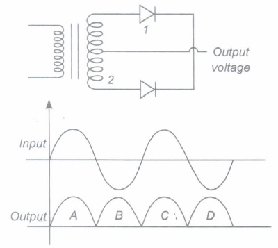
A,C
B, D
B, C
A, D
13.
In the half-wave rectifier circuit shown. Which one of the following waveforms is true for VCD the output across C and D?
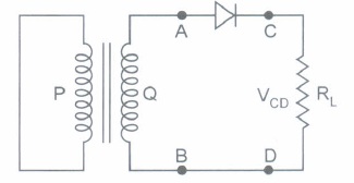
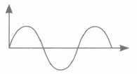
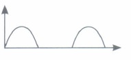
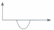
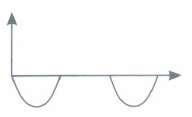
14.
The forbidden energy band gap in conductors, semiconductors and insulators are EG1, EG2 and EG3 respectively. The relation among them is
EG1 = EG2 = EG3
EG1 < EG2 < EG3
EG1 > EG2 > EG3
EG1 < EG2 > EG3
15.
Electrical conductivity of a semiconductor
decreases with the rise in its temperature.
increases with the rise in its temperature
does not change with the rise in its temperature.
first increases and then decreases with the rise in its temperature
16.
The output of the given circuit in figure is given below.
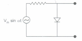
would be zero at all times.
would be like a half-wave rectifier with positive cycles in output.
would be like a half-wave rectifier with negative cycles in output.
would be like that of a full-wave rectifier.
17.
In figure given, assuming the diodes to be ideal
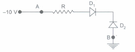
D1 is forward biased and D2 is reverse biased and hence current flows from A to B.
D2 is forward biased and D1 is reverse biased and hence no current flows from B to A and vice versa.
D1 and D2 are both forward biased and hence current flows from A to B.
D1 and D2 are both reverse biased and hence no current flows from A to B and vice versa
18.
A photodiode converts
variation in intensity of light into current amplitude variation
variation of current amplitude into variation in intensity of emitted light
variation of voltage into variation of current
variation of intensity of light into variation of volume
19.
The current through an ideal p-n junction shown in the following circuit diagram will be
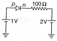
zero
1 mA
10 mA
30 mA
20.
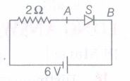
The diode shown in the circuit is a silicon diode. The potential difference between the points A and B will be
6 V
0.6 V
0.7 V
0 V
21.
Which is reverse biased diode?
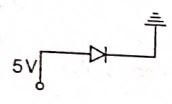
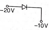
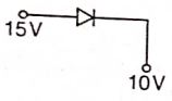
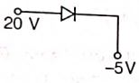
22.
If reverse biasing potential is increased beyond a certain critical (breakdown) value, then
diode gets destroyed due to overheating
no current flows through the diode
after breakdown a heavy current flows from n to p side
potential barrier becomes zero
23.
Which of these graphs shows potential difference between p-side and n-side of a p-n Junction in equilibrium?
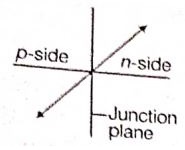
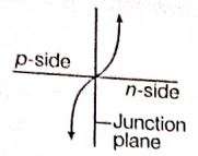
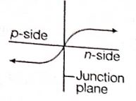
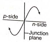
24.
The potential barrier of germanium diode is
0.1 V ,
0.3 V
0.5 V
0.7 V
25.
In an n-type silicon, which of the following statements is correct?
Electrons are majority charge carriers and trivalent atoms are the dopants
Electrons are minority charge carriers and pentavalent atoms are the dopants
Holes are minority charge carriers and pentavalent atoms are the dopants
Holes are majority charge carriers and trivalent atoms are the dopants
26.
The ratio of output frequencies of half wave rectifier and a full-wave rectifier, when an input of frequency 200 Hz is fed at input ?
1 :2
2:1
4:1
1:4
27.
A 220 V AC supply is connected between points A and B (figure). What will be the potential difference V across the capacitor?
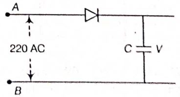
220 V
110 V
0 V
\(220 \sqrt{2} \mathrm{~V}\)
28.
The substance which is doped in an intrinsic semiconductor to make p-type semiconductor is
phosphorus
antimony
aluminium
arsenic
29.
The lighting emitting diode(LED),
is made from the semiconducting compound gallium arsenide phosphide
emits light when forward biased
is made from one of the two basic semiconducting materials,silicon or germanium
emits light when reverse biased.
30.
Which of the following statements concerning the depletion zone of an unbiased p-n junction is (are) true?
The width of the zone is independent of the densities of the dopants(impurities)
The width of the zone is dependent on the densities of the dopants
The electric field in the zone is provided by the electrons in the conduction band and holes in the valence band
The electric field in the zone is produced by the ionized dopant atoms.
31.
For an intrisnsic semiconductor the staement/ statements that hold good are:
an intrinsic semiconductor is a perfect insulator at 0 K
the number of charge carriers varies with temperature in an exponential way.
the number density of electrons is always more than the number density of holes.
the mobility of electrons is more than that of holes.
32.
The electrical conductivity of pure silicon can be increased by
increasing the temperature
doping donor impurities
doping acceptor impurities
falling ultraviolet light on it
33.
The number of minority carriers crossing the junction of a diode depends primarily on the
concentration of doping impurities
imagnitude of potential barrier
magnitude of the forward bias voltage
rate of thermal generation of electron-hole pair
34.
The barrier potential of a p-n junction depends on :
(i) type of semiconductor material
(ii) amount of doping
(iii) temperature.
Which one of the following is correct?
(i) and (ii) only
(ii) only
(ii) and (iii) only
(i),(ii) and (iii)
35.
A \(p-n\) junction diode having potential difference 0.5 volt across its junction which does not depend on current, is connected in series with resistance of 20 \(\Omega \)across source. If 0.1 A current passes through resistance, then what is the voltage of the source.
1.5 V
2.0 V
2.5 V
5 V
36.
In n type semiconductor when all donor states are filled,then the net charge density in the donor states becomes
1
>1
<1,but not zero
zero
37.
Pure Si at 500 k has equal number of electron \((n_{ e })\)and hole \((n_{ h })\)concentration of \(1.5\times10^{ 16 }m^{ -3 }\) Doping by indium increases \({ n }_{ h }\) to \(4.5\times10^{ 22 }m^{ -3 }\)
n - type with electron concentration \({ n }_{ e }=5\times10^{ 22 }m^{ -3 }\)
p-type with electron concentration \({ n }_{ e }=2.5\times10^{ 10 }m^{ -3 }\)
\(n-\)type with electron concentration \({ n }_{ e }=2.5\times10^{ 23 }m^{ -3 }\)
\(p-\) type having electron concentration \({ n }_{ e }=5\times10^{ 9 }m^{ -3 }\)
38.
A Ge specimen is doped with AI. The concentration of acceptor atoms is \(-10^{ 21 }\) atoms/\(m^{ 3 }\) , the concentration of electrons in the specimen is
\(10^{ 17 }/m^{ 3 }\)
\(10^{ 15 }/m^{ 3 }\)
\(10^{ 4 }/m^{ 3 }\)
\(10^{ 2 }/m^{ 3 }\)
39.
A semiconductor has an electron concentration \(8 \times 10^{ 13 }\ per\ m^{ 3 }\) and hole concentration of \(5\times10^{ 12 }\ per\ m^{ 3 }\). The semiconductor is
n - type
p - type
Intrinsic semiconductor
None of the above
40.
The energy gap between conduction band and valence band is of the order of 0.07 eV. It is a/an
insulator
conductor
semiconductor
alloy
41.
The resistance of an intrinsic semi-conductor when heated
increases
remains constant
decreases linearly
decreases exponentially
42.
The breakdown in a reverse biased p-n junction is more likely to occur due to
large velocity of the minority charge carriers if the doping concentration is small
large velocity of the minority charge carriers if the doping concentration is large
strong electric field in a depletion region if the doping concentration is small
strong electric field in the depletion region if the doping concentration is large
43.
In the depletion region of a diode
there are no mobile charges
equal number of holes and electrons exist, making the region neutral
recombination of holes and electrons has taken place
mmobile charged ions exist
44.
When an electric field is applied across a semiconductor
electrons move from lower energy level to higher energy level in the condition band
electrons move from higher energy level to lower energy level in the conduction band
holes in the valence band move from higher energy level to lower energy level
holes in the valence band move from lower energy level to higher energy level.
45.
Hole is
an anti-particle of electron
a vacancy created when an electron leaves a covalent bond
absence of free electron
an artificially created particle
46.
The conductivity of a semiconductor increases with increase in temperature because
number density of free current carriers increases
relaxation time increases
both number density of carriers and relaxation time increase
number density of carriers increases, relaxation time decreases but effect of decrease in relaxation time is much less than increase in number density
47.
When a forward bias is applied to p-n junctions it
raises the potential barrier
reduces the majority carrier to zero
lower the potential barrier
None of these
48.
In an unbiased p-n junction, holes diffuse from the p- region to n- region because
Free electrons in the n-region attract them
they move across the junction by the potential difference
hole concentration in p-region is more as compared to hole concentration in n-region
all the above
49.
Carbon, silicon and germanium have four valence electrons each, These are characterised by valence and conduction bands separated by energy bandgap respectively equal to \((E_{ g })_{ c, }({ E }_{ g })_{ si }\ and\ { (E }_{ g })_{ Ge }\)Which of the following statements is true?
\((E_{ g })_{ si, }<({ E }_{ g })_{ Ge }<\ { (E }_{ g })_{ C }\)
\((E_{ g })_{ C, }>({ E }_{ g })_{ si }>\ { (E }_{ g })_{ Ge }\)
\((E_{ g })_{ C, }=({ E }_{ g })_{ si }=\ { (E }_{ g })_{ Ge }\)
\((E_{ g })_{ C, }=({ E }_{ g })_{ si }=\ { (E }_{ g })_{ Ge }\)
50.
In n-type silicon, Which of the following statement is true:
Electrons are majority carriers and trivalent atoms are the dopants
Electrons are minority carriers and pentavalent atoms are the dopants
Holes are minority carriers and pentavalent atoms are the dopants
Holes are majority carriers and trivalent atoms are the dopants.
51.
The built in potential of p-n junction diode is a function of
temperature
biased voltage
doping density
all of the above
52.
The electrical resistance of depletion layer is large because
it has no charge carriers
it has few holes as charge carriers
it contains few electrons as charge carriers
it contains few ions as charge carriers
53.
In the middle of the depletion layer of a review biased p-n junction, the
electric field is zero
potential is zero
electric field is maximum
potential is maximum
54.
The reverse saturation of p-n junction
depends on doping concentration
depends on diffusion lengths of carriers
depends on the doping concentrations and diffusions lengths
depends on the doping concentartions, diffusion length and device temperature
55.
A semiconductor is cooled from \(T_{ 1 }K\ to\ T_{ 2 }k\) Its resistance will
decrease
increase
first decreases then increases
will not change
56.
Which type of semiconductor is obtained by mixing arsenic with silicon?
\(n-type\)
\(p-type\)
Both
None
57.
A p-type semiconductor is obtained by doping silicon with
germanium
gallium
bismuth
Phosphorus
58.
n - type semiconductor is obtained when
germanium is doped with arsenic
germanium is doped with indium
germanium is doped with aluminium
silicon is doped with indium
59.
In an n-type semiconductor, the Fermi level lies 0.3 e V below the conduction band at 300 k. If the temperature is increased to 330 k, where does the new position of the Fermi level lie?
0.55 e V below the conduction band
0.44 eV below the conduction band
0.33 eV below the conduction band
0.27 eV below the conduction band
60.
In intrinsic semiconductor at room temperature, the number of electrons and holes are
equal
zero
unequal
infinite
61.
In good conductorsof electricity the type of bonding that exists is
ionic
vander waals
covalent
metallic
62.
The conduction band in a solid is partially filled at 0 k. The solid sample is
Conductor
Semiconductor
Insulator
none of these
63.
64.
65.
66.
67.
68.
69.
70.
71.
72.
73.
74.
75.
76.
77.
78.
79.
80.
81.
82.
83.
Assertion (A) A rectifier converts as alternating curent into a direct curent.
Reason (R) A p-n junction diode can work as a rectifier.
(a) Both Assertion and Reason are true and Reason is the correct explanation of Assertion.
(b) Both Assertion and Reason are true but Reason is not the correct explanation of Assertion.
(c) Assertion is true but Reason is false.
(d) Assertion is false but Reason is true.
84.
Assertion (A) The resistivity of a semiconductor decreases with temperature.
Reason (R) The atoms of a semiconductor vibrate with larger amplitudes of higher temperatures thereby increasing its resistivity.
(a) Both Assertion and Reason are true and Reason is the correct explanation of Assertion.
(b) Both Assertion and Reason are true but Reason is not the correct explanation of Assertion.
(c) Assertion is true but Reason is false.
(d) Assertion is false but Reason is true.
85.
Assertion (A) The conductivity of an intrinsic semiconductor depends on its temperature.
Reason (R) The conductivity of an intrinsic semiconductor is slightly higher than that of a lightly doped p-type semiconductor.
(a) Both Assertion and Reason are true and Reason is the correct explanation of Assertion.
(b) Both Assertion and Reason are true but Reason is not the correct explanation of Assertion.
(c) Assertion is true but Reason is false.
(d) Assertion is false but Reason is true.
86.
Asseetion (A) : The half-wave rectifier work only for positive half cycle of ac.
Reason (R) : In half-wave rectifier only one diode is used.
Codes:
(a) Both A and R are true and R is the correct explanation of A
(b) Both A and R are true but R is NOT the correct explanation of A
(c) A is true but R is false
(d) A is false and R is also false
87.
Assertion (A) : V - I characteristic of p-n diode is same as that of any other conductor.
Reason (R) : p-n diode behave as conductor at room temperature.
Codes:
(a) Both A and R are true and R is the correct explanation of A
(b) Both A and R are true but R is NOT the correct explanation of A
(c) A is true but R is false
(d) A is false and R is also false
88.
Assertion (A) : The resistivity of a semiconductor increases with temperature.
Reason (R) : The atoms of a semiconductor vibrate with larger amplitude at higher temperatures thereby increasing its resistivity.
Codes:
(a) Both A and R are true and R is the correct explanation of A
(b) Both A and R are true but R is NOT the correct explanation of A
(c) A is true but R is false
(d) A is false and R is also false
89.
Assertion (A) : At 0 K, Germanium is a superconductor.
Reason (R) : At 0 K, Germanium offers zero resistance.
Codes:
(a) Both A and R are true and R is the correct explanation of A
(b) Both A and R are true but R is NOT the correct explanation of A
(c) A is true but R is false
(d) A is false and R is also false
90.
Assertion (A) : At absolute zero the conductivity of semiconductor is zero.
Reason (R) : In a semiconductor there are no free electrons at any temperature.
Codes:
(a) Both A and R are true and R is the correct explanation of A
(b) Both A and R are true but R is NOT the correct explanation of A
(c) A is true but R is false
(d) A is false and R is also false
91.
Assertion (A) : Diamond behaves like an insulator.
Reason (R) : There is a large energy gap between valence band and conduction band of diamond.
Codes:
(a) Both A and R are true and R is the correct explanation of A
(b) Both A and R are true but R is NOT the correct explanation of A
(c) A is true but R is false
(d) A is false and R is also false
92.
Assertion (A) : The depletion layer in the p-n junction is free from mobile charge carriers.
Reason (R) : There is no electric field across the junction barrier.
Codes:
(a) Both A and R are true and R is the correct explanation of A
(b) Both A and R are true but R is NOT the correct explanation of A
(c) A is true but R is false
(d) A is false and R is also false
1.
(d)
diffusion current remains almost constant but drift current increases till both currents-become equal
2.
(c)
the potential barrier is raised
3.
(b)
diffusion of the electrons and holes
4.
(c)
5 x 10⁹ m-3
5.
(b)
0.25 Ω
6.
(c)
7.
(b)
5/50 A
8.
(a)
0.2 A
9.
(b)
absence of one electron
10.
(b)
gallium to pure silicon
11.
(b)
2.3 V
12.
(b)
B, D
13.
(b)
14.
(b)
EG1 < EG2 < EG3
15.
(b)
increases with the rise in its temperature
16.
(c)
would be like a half-wave rectifier with negative cycles in output.
17.
(b)
D2 is forward biased and D1 is reverse biased and hence no current flows from B to A and vice versa.
18.
(a)
variation in intensity of light into current amplitude variation
19.
(a)
zero
20.
(a)
6 V
21.
(b)
22.
(c)
after breakdown a heavy current flows from n to p side
23.
(c)
24.
(b)
0.3 V
25.
(c)
Holes are minority charge carriers and pentavalent atoms are the dopants
26.
(a)
1 :2
27.
(d)
\(220 \sqrt{2} \mathrm{~V}\)
28.
(c)
aluminium
29.
(a)
is made from the semiconducting compound gallium arsenide phosphide
30.
(a)
The width of the zone is independent of the densities of the dopants(impurities)
31.
(b)
the number of charge carriers varies with temperature in an exponential way.
32.
(a)
increasing the temperature
33.
(d)
rate of thermal generation of electron-hole pair
34.
(d)
(i),(ii) and (iii)
35.
(c)
2.5 V
36.
(b)
>1
37.
(d)
\(p-\) type having electron concentration \({ n }_{ e }=5\times10^{ 9 }m^{ -3 }\)
38.
(a)
\(10^{ 17 }/m^{ 3 }\)
39.
(a)
n - type
40.
(b)
conductor
41.
(d)
decreases exponentially
42.
(a)
large velocity of the minority charge carriers if the doping concentration is small
43.
(a)
there are no mobile charges
44.
(a)
electrons move from lower energy level to higher energy level in the condition band
45.
(b)
a vacancy created when an electron leaves a covalent bond
46.
(d)
number density of carriers increases, relaxation time decreases but effect of decrease in relaxation time is much less than increase in number density
47.
(b)
reduces the majority carrier to zero
48.
(c)
hole concentration in p-region is more as compared to hole concentration in n-region
49.
(b)
\((E_{ g })_{ C, }>({ E }_{ g })_{ si }>\ { (E }_{ g })_{ Ge }\)
50.
(c)
Holes are minority carriers and pentavalent atoms are the dopants
51.
(d)
all of the above
52.
(a)
it has no charge carriers
53.
(a)
electric field is zero
54.
(d)
depends on the doping concentartions, diffusion length and device temperature
55.
(b)
increase
56.
57.
(b)
gallium
58.
(a)
germanium is doped with arsenic
59.
(d)
0.27 eV below the conduction band
60.
equal
61.
(d)
metallic
62.
Conductor
63.
64.
65.
66.
67.
68.
69.
70.
71.
72.
73.
74.
75.
76.
77.
78.
79.
80.
81.
82.
83.
(c) Assertion is true but Reason is false.
84.
(c) Resistivity of a semiconductor decreases with the temperature. The atoms of a semiconductor vibrate with larger amplitudes at higher temperature thereby increasing its conductivity not resistivity.
85.
(c) The conductivity of an intrinsic semiconductor is less than that of a lightly doped p-type semiconductor.
86.
(a): In half wave rectifier, the one diode is biased only when ac is in positive half of its cycle.For negative half of the ac cycle the diode is reversed biased and there is no output corresponding to that. Since for only one-half cycle we get a voltage output,because of which it is called half wave rectifier.
87.
(d) : The V-I characteristic of p-n diode depends whether the junction is forward biased or reverse biased. This can be showed by graph between voltage and current.
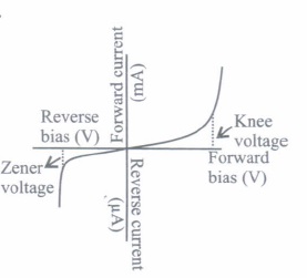
In the given graph knee voltage is a voltage at which forward bias becomes greater than the potential barrier, the forward current increases almost linearly, where as zener voltage is a voltage at which reverse current increases suddenly. From this graph we can verify that p-n diode characteristics are very different from that of conductor which obey's Ohm's law.
88.
(d) : With the increase of temperature, the average energy exchanged in a collision increases and so more valence electrons can cross the energy gap, thereby increasing the electron-hole pairs. As in a semiconductor, conduction occurs mainly through electron-hole pairs, so conductivity increases with increase of temperature. Which in turn implies that the resistivity of a semiconductor decreases with rise in temperature.
89.
(d) : At 0 K, Germanium offers infinite resistance, and it behaves as an insulator
90.
(c): In a semiconductor, there are no free electrons at 0 K. The number of free electrons increases with increase in temperature because with increase in temperature the electron get sufficient energy to cross forbidden band and reach conduction band. But total number of free electrons in a semiconductor is less than that in a conductor.
91.
(a): In insulator, the forbidden energy gap is quite large. When electric field is applied to such a solid, the electron find it difficult to acquire such a large amount of energy. Thus no electron flow occurs.
92.
(c): Due to diffusion of holes from the p-region to the n-region and of electrons from the n-region to the p-region an electric field is set up across the junction barrier. Once the depletion layer is formed it is in equilibrium and becomes free of mobile charge carriers.

12th Standard CBSE Syllabus & Materials
12th Standard CBSE
CBSE 12th Computer Science Python Revision Tour I - New Previous year Question Papers Study Material - QB365 Set A
NEW12th Standard CBSE
CBSE 12th Business Studies Planning Important Questions And Answers Study Material - QB365 Set A
NEW12th Standard CBSE
CBSE 12th Business Studies Business Environment Important Questions And Answers Study Material - QB365 Set A
NEW12th Standard CBSE
CBSE 12th Business Studies Principles of Management Important Questions And Answers Study Material - QB365 Set A



NCERT Books

Syllabus

Exam Pattern

Sample Question Papers

Previous year Question Papers

Important Notes

MCQ Practice test

NCERT Exemplers

Case study Questions

Image Based Questions

Passage based Questions

HOT Questions

Value Based Questions

Model Questions Papers
NCERT ( Book Back ) Questions

Assertion and Reason
Important Questions And Answers

CBSE 12th Standard CBSE Subjects
CBSE Standards