100% FREE ACCESS
12th Standard CBSE Syllabus & Materials
12th Standard CBSE
CBSE 12th Economics Government Budget and the Economy Previous year Question Papers Study Material - QB365 Set A
NEW12th Standard CBSE
CBSE 12th Computer Science Interface Python with MySQL - New Previous year Question Papers Study Material - QB365 Set A
NEW12th Standard CBSE
CBSE 12th Computer Science Database Concept - New Previous year Question Papers Study Material - QB365 Set A
NEW12th Standard CBSE
CBSE 12th Computer Science Data Communication - New Previous year Question Papers Study Material - QB365 Set A
NEW12th Standard CBSE
CBSE 12th Computer Science Data Structures - New Previous year Question Papers Study Material - QB365 Set A
NEW12th Standard CBSE
CBSE 12th Computer Science Functions - New Previous year Question Papers Study Material - QB365 Set A

Published on: 07/03/2026
Download CBSE Class 12th Standard CBSE Physics question papers, sample papers, important questions, and previous year solved papers in PDF format. Get free study materials, NCERT solutions, and exam preparation resources for Class 12th Standard CBSE Physics
Questions + Answers key
Take MCQ Physics Test
1.
C,Si and Ge have same lattice structure. Why is C insulator while Si and Ge intrinsic semiconductor?
2.
Why is \(n\)-type semiconductor of Ge so called?
3.
What is fermi level and fermi energy?
4.
Can we take one slab of p-type semiconductor and physically join it to another n-type semiconductor to get p-n junction?
5.
Suppose a pure Si crystal has \(5\times 10^{ 28 }\) atmos \(m^{ -3 }\). It is doped by ppm concentration of pentavalent As. Calculate the number of electrons and holes. Given that \({ n }_{ i }=1.5\times { 10 }^{ 16 }m^{ 3 }\)
6.
When a forward bias applied to a p-n junction, it
(a) raises the potential barrier
(b) reduces the majority carrier current to zero
(c) lowers the potential barrier
(d) None of the above
7.
In the circuit containing an ideal p-n junction diode D and a resistor R is given an input square wave as shown
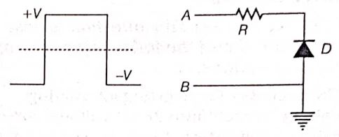
(i) What is the shape of the output waveform across diode D?
(ii) Give an explanation for your answer in part (ii)
8.
Explain the property of a p-n junction which makes it suitable for rectifying alternating voltages. Differentiate between a half-wave and a full-wave rectifier.
9.
Carbon, silicon and germanium have four valence electrons each. These are characterised by valence and conduction bands separated by energy band gap respectively equal to (Eg) C, (Eg) Si and (Eg) Ge. Which of the following statements is true?
\(\text { (a) }\left(E_{g}\right)_{\mathrm{Si}}<\left(E_{g}\right)_{\mathrm{Ge}}<\left(E_{g}\right)_{\mathrm{C}}\)
\(\text { (b) }\left(E_{g}\right)_{\mathrm{C}}<\left(E_{g}\right)_{\mathrm{Ge}}>\left(E_{g}\right)_{\mathrm{Si}}\)
\(\text { (c) }\left(E_{g}\right)_{\mathrm{C}}>\left(E_{g}\right)_{\mathrm{Si}}>\left(E_{g}\right)_{\mathrm{Ge}}\)
\(\text { (d) }\left(E_{g}\right)_{\mathrm{C}}=\left(E_{g}\right)_{\mathrm{Si}}=\left(E_{g}\right)_{\mathrm{Ge}}\)
10.
Which of the statements given In an n-type silicon, which of the following statement is true for p-type semiconductos.
(a) Electrons are majority carriers and trivalent atoms are the dopants.
(b) Electrons are minority carriers and pentavalent atoms are the dopants.
(c) Holes are minority carriers and pentavalent atoms are the dopants.
(d) Holes are majority carriers and trivalent atoms are the dopants.
11.
In half wave rectification , what is the output frequency if the input frequency is 50 Hz. What is the output frequency of a full wave rectification for the same input frequency.
12.
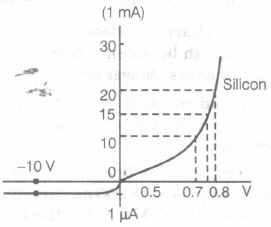
The V-I characteristic of a silicon diode is as shown in the figure. Calculate the resistance of the diode at
(i) I = 15 mA and
(ii) V = -10 V
13.
Find the binary number of \({ \left( 23.50 \right) }_{ 10}\)
14.
In the circuit \({ V }_{ s }=0.2\ V,{ V }_{ 0 }=-10V\). Find \({ V }_{ e }\), Gain \({ A }_{ u }=\frac { { V }_{ 0 } }{ V_{ c } } \) and \({ A }_{ 0 }=\frac { { V }_{ 0 } }{ V_{ s } } \)
15.
In a common emitter configuration \({ I }_{ e }=13.5mA\) , \(\\ { I }_{ b }=150\mu A\). Compute \({ I }_{ e }\) and \(\beta \).
16.
Find the value of \(\beta \), if the value of \(a\) is 0.95.
17.
Sanjay was prparing an electronic project for science exhibition. He required to light the LED using a 6 V supply. LEDs need only a very small current to make them light and they do not heat up in use. So he put a resistor in series to limit the current. Then there would be p.d. of 4 V across the resistor as there is always 2.0 V across the LED itself when it is conducting. The current should be 10 mA through both LED and the resistor. He could use the resistance by equation, R = V/I to calculate the value of R.
\(R=\frac { V }{ I } =\frac { 4V }{ 10mA } =\frac { 4V }{ 0.01A } =400V\)
Thus the protecting resistor should be around \(400\Omega \)
A semiconductor has equal electron and hole concentration of \(6\times 10^{ 8 }/{ m }^{ 3 }\). On doping with certain impurity, electron concentration increase to \(9\times { 10 }^{ 12 }/{ m }^{ 3 }\)
18.
You are given the two circuits as shown in Fig. Show that circuit (a) acts as OR gate while the circuit (b) acts as AND gate.

19.
A p-n photodiode is fabricated from a semiconductor with band gap of 2.8 eV. Can it detect a wavelength of 6000 nm?
20.
The number of silicon atoms per m3 is 5 x 1028. This is doped simultaneously with 5 x 10²² atoms per m3 of Arsenic and 5 x 10²⁰ atoms per m3 of Indium. Calculate the number of electrons and holes. Given that ni = 1.5 x 10¹⁶ m–3. Is the material n-type or p-type?
21.
The electron mobility characterises how quickly an electron can move through a metal of semiconductor when pulled by an electric field. There is an analogous quality for holes, called hole mobility. A block of pure silicon at 300 K has a length of 10 cm and an area of 1.0 cm2. A battery of emf 2 V is connected across it. The mobility of electron is 0.14 m2 y-1 s-1 and their number density is 1.5 x 10¹⁶ m-3. The mobility of holes is 0.05 m2 y-1 s-1.
(i) The electron current is
| (a) 6.72 x 10⁻⁴ A | (b) 6.72 x 10⁻⁵ A | (c) 6.72 x 10⁻⁶ A | (d) 6.72 x 10⁻⁷ A |
(ii) The hole current is
| (a) 2.0 x 10⁻⁷ A | (b) 2.2 x 10⁻⁷ A | (c) 2.4 X 10⁻⁷ A | (d) 2.6 x 10⁻⁷ A |
(iii) The number density of donor atoms which are to be added up to pure silicon semiconductor to produce an n-type semiconductor of conductivity 6.4 \(\Omega\)-1 cm-1 is approximately (neglect the contribution of holes to conductivity)
| (a) 3 x 10²² m-3 | (b) 3 x 10²³ m-3 | (c) 3 x 1024 m-3 | (d) 3 x 10²¹ m-3 |
(iv) When the given silicon semiconductor is doped with indium, the hole concentration increases to 4.5 x 10²³ m-3. The electron concentration in doped silicon is
| (a) 3 x 10⁹ m-3 | (b) 4 x 10⁹ m-3 | (c) 5 x 10⁹ m-3 | (d) 6 x 10⁹ m-3 |
(v) Pick out the statement which is not correct.
| (a) At a low temperature, the resistance of a semiconductor is very high. |
| (b) Movement of holes is restricted to the valence band only |
| (c) Width of the depletion region increases as the forward bias voltage increases in case of a p- n junction diode. |
| (d) In a forward bias condition, the diode heavily conducts |
22.
Rectifier is a device which is used for converting alternating current or voltage into direct current or voltage. Its working is based on the fact that the resistance of p-n junction becomes low when forward biased and becomes high when reverse biased. A half-wave rectifier uses only a single diode while a full wave rectifier uses two diodes as shown in figures (a) and (b) .
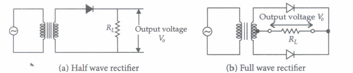
(i) If the rms value of sinusoidal input to a full wave rectifier is \(\frac{V_{0}}{\sqrt{2}}\) then the rms value of the rectifier's output is
| \(\text { (a) } \frac{V_{0}}{\sqrt{2}}\) | \(\text { (b) } \frac{V_{0}^{2}}{\sqrt{2}}\) | \(\text { (c) } \frac{V_{0}^{2}}{2}\) | \(\text { (d) } \sqrt{2} V_{0}^{2}\) |
(ii) In the-diagram, the input ac is actoss the terminals A and C. The output across Band D is
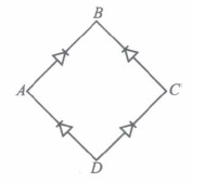
| (a) same as the input | (b) half wave rectified | (c) zero | (d) full wave rectified |
(iii) A bridge rectifier is shown in figure. Alternating input is given across A and C. If output is taken across BD, then it is
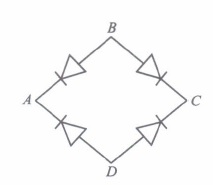
| (a) zero | (b) same as input | (c) half wave rectified | (d) full wave rectified |
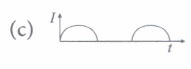
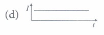
(iv) A p-n junction (D) shown in the figure can act as a rectifier. An alternating current source (V) is connected in the circuit. The current (I) in the resistor(R) can be shown by
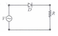
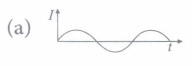 |
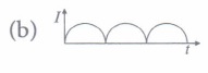 |
 |
 |
(v) With an ac input from 50 Hz power line, the ripple frequency is
| (a) 50 Hz in the dc output of half wave as well as full wave rectifier |
| (b) 100 Hz in the de output of half wave as well as full wave rectifier |
| (c) 50 Hz in the de output of half wave and 100 Hz in dc output offull wave rectifier |
| (d) 100 Hz in the dc output of half wave and 50 Hz in the de output of full wave rectifier |
1.
The 4 bonding electrons of C, Si or Ge lie, respectively, in the second, third and fourth orbit. Hence, energy required to take out an electron from these atoms (i.e., ionisation energy Eg) will be least for Ge, followed by Si and highest for C. Hence, number of free electrons for conduction in Ge and Si are significant but negligibly small for C.
2.
Because in n-type semiconductor, electrons (having negative charge) are majority carriers which are responsible for the conduction
3.
In an energy band, the highest energy level occupied by electron at 0K is called fermi level and its energy is called fermi -energy.
4.
No. Any slab, howsoever flat, will have roughness much larger than interatomic crystal spacing \((2\ to\ 3\overset { \circ }{ A } )\), so continuous contact at the atomic level is not possible.
5.
Note that thermally generated electrons (ni ~1016m–3) are negligibly small as compared to those produced by doping.
Therefore, ne \(\approx\) ND
Since ne nh = \(n_{i}^{2}\) , The number of holes
nh = (2.25 x 1032 ) / (5 x10²²)
= ~ 4.5 x 10⁹ m–3
6.
The correct statement is (c).
When a forward bias is applied to a p-n junction, it lowers the value of potential barrier. In the case of a forward bias, the potential barrier opposes the applied voltage. Hence, the potential barrier across the junction gets reduced.
7.
(i)
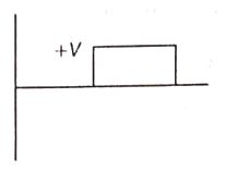
(ii) When the input voltage is negative, then it would be forward bias for diode. So, waveform would pass through the diode and we get no voltage on output. If input voltage is positive, then diode is in reverse bias and behaves as a open circuit. Now, input wave form is passed to the output terminals.
8.
The property of a p-n junction that makes it suitable for rectifying alternating voltages is its ability to act as a diode, allowing current flow in only one direction. This property is a result of the fornnations of a depletion region at the interface between the p-type and n-type semi-conductor which acts as a barrier for the flow of current in one direction making the p-n junction a useful device for rectifying AC signals.
For the difference between half wave and a full wave rectifier,
| Half-wave rectifier | Full-wave rectifier |
| Only one diode is used. | Two or four diodes are used. |
| Only one-half cycle of input ac is rectified. | Both the half cycles of input ac are rectified. |
9.
The correct statement is (c).
Of the three given elements, the energy band gap of carbon is the maximum and that of germanium is the least.
The energy band gap of these elements are related as: (Eg)C > (Eg)Si > (Eg)Ge
10.
The correct statement is (d).
In a p-type semiconductor, the holes are the majority carriers, while the electrons are the minority carriers. A p-type semiconductor is obtained when trivalent atoms, such as aluminium, are doped in silicon atoms.
11.
Given, input frequency = 50 Hz
For a half-wave rectifier, the output frequency is equal to the input frequency.
\(\therefore\) Output frequency = 50 Hz
For a full-wave rectifier, the output frequency is twice the input frequency.
\(\therefore\) Output frequency = 2 x 50 = 100 Hz.
12.
Considering the diode characteristics as a straight line between I = 10 mA to I = 20 mA passing through the origin, we can calculate the resistance using Ohm’s law.
(a) From the curve, at I = 20 mA, V = 0.8 V, I = 10 mA, V = 0.7 V
\(r_{f b}=\Delta V / \Delta I=0.1 \mathrm{~V} / 10 \mathrm{~mA}=10 \ \Omega\)
(b) From the curve at V = –10 V, I = –1 \(\mu\) A,
Therefore,
\(r_{r b}=10 \mathrm{~V} / 1 \mu \mathrm{A}=1.0 \times 10^{7} \ \Omega\)
13.
\({ \left( 10111.10 \right) }_{ 2 }\)
14.
\({ V }_{ c }={ V }_{ s }+{ V }_{ F }={ V }_{ s }+\frac { { V }_{ 0 } }{ 100 } \)
or
\({ V }_{ c }=0.2+\frac { -10 }{ 100 } \)
\(=0.2-0.1=0.1\)
\({ A }_{ 0 }=\frac { { V }_{ 0 } }{ { V }_{ c } } =\frac { -10 }{ 0.1 } =\frac { -10 }{ 0.1 } =-100\)
\({ A }_{ 0 }=\frac { -10 }{ 0.2 } =-50\)
15.
\(\beta =\frac { { I }_{ c } }{ { I }_{ b } } =\frac { 13.5 }{ 150\times 10^{ -3 } } =90\)
And \({ I }_{ e }={ I }_{ b }+{ I }_{ c }=13.5+150\times { 10 }^{ -3 }\)
\(=13.5+0.15\)
or \({ I }_{ e }=13.65 \ mA\)
16.
Given \(a\)= 0.95
So
\(\beta =\frac { a }{ 1-a } =\frac { 0.95 }{ 1-0.95 }\)
\(=\frac { 95 }{ 5 } =19\).
17.
(i) New semiconductor must be n-type, because the electron concentration increases.
(ii) Given,
\({ n }_{ i }=6\times 10^{ 8 }/{ m }^{ 3 }\)
\(\\ { n }_{ e }=9\times { 10 }^{ 12 }/{ m }^{ 3 }\)
\(\\ { n }_{ e }{ n }_{ h }={ n }_{ i }^{ 2 }\)
\(\\ \Rightarrow { n }_{ h }=\frac { { n }_{ i }^{ 2 } }{ { n }_{ e } } =\frac { (6\times 10^{ 8 })^{ 2 } }{ 9\times { 10 }^{ 12 } } \)
\(\\ =\frac { 36\times { 10 }^{ 16 } }{ 9\times 10^{ 12 } } \)
\(\\ =4\times 10^{ 4 }/{ m }^{ 3 }\)
18.
(a) Split the gate,
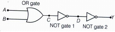
The truth table for the given circuit is as shown below:
| A | B | C | D | Y |
| 0 | 0 | 0 | 1 | 0 |
| 0 | 1 | 1 | 0 | 1 |
| 1 | 0 | 1 | 0 | 1 |
| 1 | 1 | 1 | 0 | 1 |
Here, for given A and B as inputs, C is the output of OR gate and input of NOT gate 1, D is the output of NOT gate 1 and input of NOT gate 2, then Y is finally output.
| A | B | Y |
| 0 | 0 | 0 |
| 0 | 1 | 1 |
| 1 | 0 | 1 |
| 1 | 1 | 1 |
This is same as OR gate. So, this circuit acts as OR gate.
19.
Energy band gap of the given photodiode, Eg = 2.8 eV
Wavelength, λ = 6000 nm = 6000 x 10−9 m
The energy of a signal is given by the relation:
\(E=\frac{h c}{\lambda}\)
Where
h = Planck’s constant
= 6.626 x 10⁻³⁴ Js
c = Speed of light
= 3 x 10⁸ m/s
\(E=\frac{6.626 \times 10^{-34} \times 3 \times 10^{8}}{6000 \times 10^{-9}}\)
= 3.313 x 10⁻²⁰ J
But 1.6 x 10⁻¹⁹ J = 1 eV
∴ E = 3.313 x 10⁻²⁰ J
\(=3.313 \times \frac{10^{-20}}{1.6 \times 10^{-19}}=0.207 \mathrm{eV}\)
The energy of a signal of wavelength 6000 nm is 0.207 eV, which is less than 2.8 eV − the energy band gap of a photodiode. Hence, the photodiode cannot detect the signal.
20.
For each atom doped with arsenic, one free electron is received. Similarly, for each atom doped of indium, a vacancy is created. So, number of free electrons introduced by pentavalent impurity is
\(N_{\mathrm{As}}=5 \times 10^{22} \mathrm{~m}^{-3}\)
The number of holes introduced by trivalent impurity added is
\(N_{\mathrm{I}}=5 \times 10^{20} \mathrm{~m}^{-3}\)
So, net number of electrons added is
ne = NAs - N1
\(\begin{aligned}
=5 \times 10^{22}-5 \times 10^{20}
\end{aligned}\)
\(\begin{aligned}
=4.95 \times 10^{22} \mathrm{~m}^{-3}
\end{aligned}\)
We know that, \(n_e n_h=n_i^2\)
So, \(n_h=\frac{n_i^2}{n_e}=\frac{\left(1.5 \times 10^{16}\right)^2}{4.95 \times 10^{22}}\)
\(=4.54 \times 10^9 \mathrm{~m}^{-3}\)
As, ne > nh (number of holes). So, the material is n-type semiconductor.
21.
(i) (d): \(E=\frac{V}{l}=\frac{2}{0.1}=20 \mathrm{~V} / \mathrm{m} ;\)
\(A=1.0 \mathrm{~cm}^{2}=1.0 \times 10^{-4} \mathrm{~m}^{2}\)
\(\begin{array}{l}
v_{e}=\mu_{e} E=0.14 \times 20=2.8 \mathrm{~m} \mathrm{~s}^{-1} \\
I_{e}=n_{e} A e v_{e}
\end{array}\)
\(\begin{array}{l}
=\left(1.5 \times 10^{16}\right) \times\left(1.0 \times 10^{-4}\right) \times\left(1.6 \times 10^{-19}\right) \times 2.8 \\
=6.72 \times 10^{-7} \mathrm{~A}
\end{array}\)
(ii) (c): In a pure semiconductor,
\(n_{e}=n_{h}=1.5 \times 10^{16} \mathrm{~m}^{-3}\)
\(\begin{array}{l}
v_{h}=\mu_{h} \times E=0.05 \times 20=1.0 \mathrm{~ms}^{-1} \\
I_{h}=n_{h} \mathrm{Aev}_{h}
\end{array}\)
\(\begin{array}{l}
=\left(1.5 \times 10^{16}\right) \times\left(1.0 \times 10^{-4}\right) \times\left(1.6 \times 10^{-19}\right) \times 1.0 \\
=2.4 \times 10^{-7} \mathrm{~A}
\end{array}\)
(iii) (a): \(\sigma=e n_{e} m_{e}\)
\(\text { or } n_{e}=\frac{\sigma}{e \mu_{e}}=\frac{6.4 \times 10^{2}}{\left(1.6 \times 10^{-19}\right) \times 0.14}\)
\(=3.14 \times 10^{22} \approx 3 \times 10^{22} \mathrm{~m}^{-3}\)
(iv) (c): \(n_{e}=\frac{n_{i}^{2}}{n_{h}}=\frac{\left(1.5 \times 10^{16}\right)^{2}}{4.5 \times 10^{22}}=5 \times 10^{9} \mathrm{~m}^{-3}\)
(v) (c): In case of a p-n junction diode, width of the depletion region decreases as the forward bias voltage increases.
22.
(i) (a) :The rms value of the output voltage at the load resistance \(V_{\mathrm{rms}}=\frac{V_{0}}{\sqrt{2}}\)
(ii) (d)
(iii) (a)
(iv) (c): The given circuit works as a half wave rectifier. In this circuit, we will get current through R when p-n junction is forward biased and no current when p-n junction is reverse biased. Thus the current (I) through resistor (R) will be shown in option (c).
(v) (c)

12th Standard CBSE Syllabus & Materials
12th Standard CBSE
CBSE 12th Computer Science Python Revision Tour I - New Previous year Question Papers Study Material - QB365 Set A
NEW12th Standard CBSE
CBSE 12th Business Studies Planning Important Questions And Answers Study Material - QB365 Set A
NEW12th Standard CBSE
CBSE 12th Business Studies Business Environment Important Questions And Answers Study Material - QB365 Set A
NEW12th Standard CBSE
CBSE 12th Business Studies Principles of Management Important Questions And Answers Study Material - QB365 Set A



NCERT Books

Syllabus

Exam Pattern

Sample Question Papers

Previous year Question Papers

Important Notes

MCQ Practice test

NCERT Exemplers

Case study Questions

Image Based Questions

Passage based Questions

HOT Questions

Value Based Questions

Model Questions Papers
NCERT ( Book Back ) Questions

Assertion and Reason
Important Questions And Answers

CBSE 12th Standard CBSE Subjects
CBSE Standards