12th Standard CBSE Syllabus & Materials
12th Standard CBSE
CBSE 12th Economics Government Budget and the Economy Previous year Question Papers Study Material - QB365 Set A
NEW12th Standard CBSE
CBSE 12th Computer Science Interface Python with MySQL - New Previous year Question Papers Study Material - QB365 Set A
NEW12th Standard CBSE
CBSE 12th Computer Science Database Concept - New Previous year Question Papers Study Material - QB365 Set A
NEW12th Standard CBSE
CBSE 12th Computer Science Data Communication - New Previous year Question Papers Study Material - QB365 Set A
NEW12th Standard CBSE
CBSE 12th Computer Science Data Structures - New Previous year Question Papers Study Material - QB365 Set A
NEW12th Standard CBSE
CBSE 12th Computer Science Functions - New Previous year Question Papers Study Material - QB365 Set A

Published on: 20/08/2026
Download CBSE Class 12th Standard CBSE Physics question papers, sample papers, important questions, and previous year solved papers in PDF format. Get free study materials, NCERT solutions, and exam preparation resources for Class 12th Standard CBSE Physics
Questions + Answers key
Take MCQ Physics Test
1.
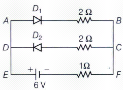
Assuming that the two diodes D1 and D2 used in the electric circuit as shown in the figure are ideal, find out the value of the current flowing through 1 \(\Omega \) resistor.
2.
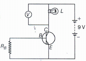
In the given circuit diagram, a voltmeter V is connected across a lamp L. How would
(i) the brightness of the lamp and
(ii) voltmeter reading V be affected, if the value of resistance RB is decreased? Justify your answer.
3.
C,Si and Ge have same lattice structure. Why is C insulator while Si and Ge intrinsic semiconductor?
4.
What is the function of base region of a transistor? Why is this region made thin and slightly doped?
5.
Would you prefer to use a transistor as a common base or a common emitter amplifier?
6.
What happens when a forward bias is applied to a \(p-n\) junction?
7.
Write the full form of the terms (i) SSI and
(ii) VLSI used for different types of integrated circuits.
8.
Write the full forms of the terms
(i) MSI and
(ii) LSI used for different types of integrated circuits.
9.
Can we take one slab of p-type semiconductor and physically join it to another n-type semiconductor to get p-n junction?
10.
Suppose a pure Si crystal has \(5\times 10^{ 28 }\) atmos \(m^{ -3 }\). It is doped by ppm concentration of pentavalent As. Calculate the number of electrons and holes. Given that \({ n }_{ i }=1.5\times { 10 }^{ 16 }m^{ 3 }\)
11.
When a forward bias applied to a p-n junction, it
(a) raises the potential barrier
(b) reduces the majority carrier current to zero
(c) lowers the potential barrier
(d) None of the above
12.
Carbon, silicon and germanium have four valence electrons each. These are characterised by valence and conduction bands separated by energy band gap respectively equal to (Eg) C, (Eg) Si and (Eg) Ge. Which of the following statements is true?
\(\text { (a) }\left(E_{g}\right)_{\mathrm{Si}}<\left(E_{g}\right)_{\mathrm{Ge}}<\left(E_{g}\right)_{\mathrm{C}}\)
\(\text { (b) }\left(E_{g}\right)_{\mathrm{C}}<\left(E_{g}\right)_{\mathrm{Ge}}>\left(E_{g}\right)_{\mathrm{Si}}\)
\(\text { (c) }\left(E_{g}\right)_{\mathrm{C}}>\left(E_{g}\right)_{\mathrm{Si}}>\left(E_{g}\right)_{\mathrm{Ge}}\)
\(\text { (d) }\left(E_{g}\right)_{\mathrm{C}}=\left(E_{g}\right)_{\mathrm{Si}}=\left(E_{g}\right)_{\mathrm{Ge}}\)
13.
Which of the statements given In an n-type silicon, which of the following statement is true for p-type semiconductos.
(a) Electrons are majority carriers and trivalent atoms are the dopants.
(b) Electrons are minority carriers and pentavalent atoms are the dopants.
(c) Holes are minority carriers and pentavalent atoms are the dopants.
(d) Holes are majority carriers and trivalent atoms are the dopants.
14.
In half wave rectification , what is the output frequency if the input frequency is 50 Hz. What is the output frequency of a full wave rectification for the same input frequency.
15.
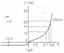
The V-I characteristic of a silicon diode is as shown in the figure. Calculate the resistance of the diode at
(i) I = 15 mA and
(ii) V = -10 V
16.
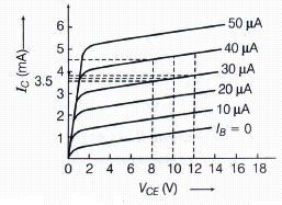
Output characteristics of an n-p-n transistor in CE configuration is shown in the figure.
Determine,
(i) dynamic output resistance (ii) DC current gain
(iii) AC current gain at an operating point VCE = 10 V, when IB = 30\(\mu\)A.
17.
Predict the effect on the electrical properties of a silicon crystal at room temperature, if every millionth silicon atom temperature, if every millionth silicon atom is replaced by an atom of indium. Given, Concentration of silicon atoms = \(5\times { 10 }^{ 28 }{ m }^{ -3 }\) intrinsic carrier concentration = \(1.5\times { 10 }^{ 16 }{ m }^{ -3 }\) He = 0.135 m3/ V-s and Hh = 0.048 m3 / V-s.
18.
What do the acronyms LASER and LED stand for? Name the factor determines
(i) frequency and
(ii) intensity of light emitted by led.
19.
The current gain in common emitter amplifier is 59.If the emitter current is 6.0 mA,find,(i) base current (ii)collector current.
20.
A semiconductor has equal electron and hole concentration of \(2\times10^{ 8 }m^{ -3 }\)
(i) What type of semiconductor is obtained on doping?
(ii) Calculate the new electron hole concentration of the semiconductor
(iii) How does the energy gap very with doping?
21.
(a) With the help of a circuit diagram, briefly explain the working of a full-wave rectifier using p-n junction diodes.
(b) Draw V-I characteristics of a p-n junction diode. Explain how these characteristics make a diode suitable for rectification.
(c) Carbon and silicon have the same lattice structure. Then, wlhy is carbon an insulator but silicon a semiconductor?
22.
(a) A germanium crystal is doped with antimony. With the help of energy-band diagram, explain how the conductivity of the doped crystal is affected.
(b) Briefly explain the two processes involved in the formation of a p-n junction.
(c) What will the effect of (I) forward biasing, and (II) reverse biasing be on the width of depletion layer in a p-n junction diode?
1.
According to the question,
D2 is in reverse bias, so it acts as open circuit
\(\begin{aligned}
R_{\mathrm{eq}} & =2+1=3 \Omega
\end{aligned}\)
\(\begin{aligned}
I & =\frac{V}{R_{\mathrm{eq}}}=\frac{6}{3}=2 \mathrm{~A}
\end{aligned}\)
2.
The given figure in question common emitter (CE) configuration of an n-p-n transistor. The base-emitter junction is forward biased and collector-base junction is reverse biased.
As, the base resistance RB decreases, the input circuit will become more forward biased thus decreasing the base current (IB ) (i.e. less number electron-hole recombination in base due to reduction in area of base) and increasing the emitter current (IE ). This will increase the collector current (IC) as IE = IB + IC .
When IC increase which flows through the lamp, the voltage across the bulb will also increase, thus making the lamp brighter and as the voltmeter is connected in parallel with the lamp, the reading in the voltmeter will also increase.
3.
The 4 bonding electrons of C, Si or Ge lie, respectively, in the second, third and fourth orbit. Hence, energy required to take out an electron from these atoms (i.e., ionisation energy Eg) will be least for Ge, followed by Si and highest for C. Hence, number of free electrons for conduction in Ge and Si are significant but negligibly small for C.
4.
In a transistor, the base region brings an interaction between emitter and collector. The base is kept thin and slightly doped so that, when emitter of transistor is forward biased, the less number of electron-hole combination takes place in base region and majority of charge carriers going from emitter towards base, pass over to collector. As a result of it, the collector current becomes quite good in comparison to base current.
5.
A common emitter transistor amplifier is preferred when we require better current gain and power gain. But common base transistor amplifier is preferred when we require better voltage gain without any phase change of signal voltage
6.
When a forward bias is applied to a p-n junction, the size of the depletion layer decreases. The resistance of the junction becomes low. The movement of the majority carriers takes place across the junction, resulting current, known as forward current which increases rapidly with increase in forward voltage.
7.
(i) SSI stands for Small Scale Integration circuits.
(ii) VLSI stands for Very Large Scale Integration circuits.
8.
(i) MSI stands for Medium Scale Integration circuits.
(ii) LSI stands for Large Scale Integration circuits.
9.
No. Any slab, howsoever flat, will have roughness much larger than interatomic crystal spacing \((2\ to\ 3\overset { \circ }{ A } )\), so continuous contact at the atomic level is not possible.
10.
Note that thermally generated electrons (ni ~1016m–3) are negligibly small as compared to those produced by doping.
Therefore, ne \(\approx\) ND
Since ne nh = \(n_{i}^{2}\) , The number of holes
nh = (2.25 x 1032 ) / (5 x10²²)
= ~ 4.5 x 10⁹ m–3
11.
The correct statement is (c).
When a forward bias is applied to a p-n junction, it lowers the value of potential barrier. In the case of a forward bias, the potential barrier opposes the applied voltage. Hence, the potential barrier across the junction gets reduced.
12.
The correct statement is (c).
Of the three given elements, the energy band gap of carbon is the maximum and that of germanium is the least.
The energy band gap of these elements are related as: (Eg)C > (Eg)Si > (Eg)Ge
13.
The correct statement is (d).
In a p-type semiconductor, the holes are the majority carriers, while the electrons are the minority carriers. A p-type semiconductor is obtained when trivalent atoms, such as aluminium, are doped in silicon atoms.
14.
Given, input frequency = 50 Hz
For a half-wave rectifier, the output frequency is equal to the input frequency.
\(\therefore\) Output frequency = 50 Hz
For a full-wave rectifier, the output frequency is twice the input frequency.
\(\therefore\) Output frequency = 2 x 50 = 100 Hz.
15.
Considering the diode characteristics as a straight line between I = 10 mA to I = 20 mA passing through the origin, we can calculate the resistance using Ohm’s law.
(a) From the curve, at I = 20 mA, V = 0.8 V, I = 10 mA, V = 0.7 V
\(r_{f b}=\Delta V / \Delta I=0.1 \mathrm{~V} / 10 \mathrm{~mA}=10 \ \Omega\)
(b) From the curve at V = –10 V, I = –1 \(\mu\) A,
Therefore,
\(r_{r b}=10 \mathrm{~V} / 1 \mu \mathrm{A}=1.0 \times 10^{7} \ \Omega\)
16.
(i) Dynamic output resistance is given as,
\({ R }_{ e }={ \left( \frac { \Delta { V }_{ CE } }{ \Delta { I }_{ C } } \right) }_{ { I }_{ B }=constant }=\frac { 12-8 }{ (3.6-3.4)\times { 10 }^{ -3 } } \)
\(\frac { 4 }{ 0.2\times { 10 }^{ -3 } } =20\kappa \Omega \)
(ii) DC current gain,
\(\beta _{ DC }=\frac { { I }_{ C } }{ { I }_{ B } } =\frac { 3.5mA }{ 30\mu A } =\frac { 3.5\times { 10 }^{ -3 } }{ 30\times { 10 }^{ -6 } } =\frac { 350 }{ 3 } =116.67\)
(iii) AC current gain,
\(\beta _{ AC }=\frac { \triangle I_{ C } }{ \triangle { I }_{ B } } =\frac { \left( 4.7-3.5 \right) mA }{ \left( 40-30 \right) \mu A } =\frac { 1.2\times { 10 }^{ -3 } }{ 10\times { 10 }^{ -6 } } =120\)
17.
As, Concentration of Si atom \(=5\times { 10 }^{ 28 }\) /m3
The doping of indium is 1 atom 106 atoms of Si. But indium has three valence electrons and each doped indium atom creates one hole in Si crystal. Hence, it acts as an acceptor atom.
Concentration of acceptor atoms,
\({ n }_{ h }=5\times { 10 }^{ 28 }\times { 10 }^{ -6 }=5\times { 10 }^{ 22 }/{ m }^{ 3 }\)
Intrinsic carrier concentration,
\({ n }_{ i }=1.5\times { 10 }^{ 16 }/{ m }^{ 3 }\)
Hole concentration is increased
\(=\frac { { n }_{ h } }{ { n }_{ i } } =\frac { 5\times { 10 }^{ 22 } }{ 1.5\times { 10 }^{ 16 } } =3.33\times { 10 }^{ 6 }\)
New electron concentration,
\({ n }_{ e }=\frac { { n }_{ i }^{ 2 } }{ { n }_{ b } } =\frac { { \left( 1.5\times { 10 }^{ 16 } \right) }^{ 2 } }{ 5\times { 10 }^{ 22 } } =0.45\times { 10 }^{ 10 }/{ m }^{ 3 }\)
Electron concentration has been reduced
\(=\frac { { n }_{ i } }{ { n }_{ e } } =\frac { 1.5\times { 10 }^{ 16 } }{ 0.45\times { 10 }^{ 10 } } =3.33\times { 10 }^{ 6 }\)/m3
This means that the hole concentration has been increased over its intrinsic concentration by the same amount with which the electron concentration has been decreased.
The conductivity of doped silicon is given by
\(\sigma =e\left( { n }_{ e }H_{ e }+{ n }_{ h }H_{ h } \right) \)
\(\\ =\quad 1.6\times { 10 }^{ -19 }\left( 0.45\times { 10 }^{ 10 }\times 0.135+5\times { 10 }^{ 22 }\times 0.048 \right)\)
= 384 S/m
Resistivity, \(\rho =\frac { 1 }{ \sigma } =\frac { 1 }{ 384 } =0.0026\Omega -m\)
Conductivity of pure Si crystal,
\(\sigma ={ en }_{ i }\left( { H }_{ e }+{ H }_{ h } \right) \)
\(\\ =1.6\times { 10 }^{ -19 }\times 1.5\times { 10 }^{ 16 }\left( 0.135+0.048 \right) \)
\(\\ =0.4392\times { 10 }^{ -3 }S/m\)
Resistivity, \(\rho =\frac { 1 }{ \sigma } =\frac { 1 }{ 0.4392\times { 10 }^{ -3 } } =2276.\Omega -m\)
Thus, we see that the conductivity of doped Si becomes much greater than its intrinsic conductivity and the resistivity has become much smaller than the intrinsic resistivity.
18.
LASER stands for light amplification by stimulated emission of Radiation.LED stands for light emitting diode.
(i) The frequency of light emitted by an LED is related to the band gap of the semiconductor used in LED i.e., a type of material used in marketing the LED.
(ii) The intensity of light emitted by LED depends upon the doping level of the semiconductor used.
19.
Here,\(\beta =59,{ I }_{ e }=6.0\quad mA\)
\(\beta =\frac { { I }_{ c } }{ { I }_{ b } } =\frac { { I }_{ e }-{ I }_{ b } }{ { I }_{ b } } =\frac { { I }_{ e } }{ { I }_{ b } } =-1\)
\( \therefore \ 59=\frac { 6 }{ { I }_{ b } } -1 \ or \ \frac { 6 }{ { I }_{ b } } =60 \ or \ { I }_{ b }=\frac { 6 }{ 60 } =0.1 \ mA\)
\( { I }_{ c }={ I }_{ e }-{ I }_{ b }=6.0-0.1=5.9\ mA\)
20.
(i) Since on doping a semiconductor, the hole concentration ( \({ n }_{ p }=4\times10^{ 10 }m^{ -3 })\) becomes greater than electron concentration \(({ n }_{ e }=2\times10^{ 8 }m^{ -3 })\)so p-type semiconductor is formed on doping.
(ii) Here
,\(n_{ 1 }=2\times10^{ 8 }m^{ -3 };\)
\( { n }_{ p }=4times10^{ 10 }m^{ -3 };{ n }_{ e }=?\)
\( { n }_{ e }=\frac { { n }_{ i } }{ n_{ p } } =\frac { (2\times10^{ 8 })^{ 2 } }{ 4\times10^{ 10 } } =10^{ 6 }m^{ -3 }\)
(iii) Energy gap decreases with doping due to formation of acceptor energy levels just above the valence band in the energy gap region.
21.
(c) Carbon is an insulator because all of its valence electrons are used up in covalent bonding, while silicon is a semiconductor because some of its valence electrons are not involved in bonding, creating a small number of free electrons in the conduction band. This slight difference in electronic configuration results in a significant difference in their electrical properties, despite having the same lattice structure.
22.

12th Standard CBSE Syllabus & Materials
12th Standard CBSE
CBSE 12th Computer Science Python Revision Tour I - New Previous year Question Papers Study Material - QB365 Set A
NEW12th Standard CBSE
CBSE 12th Business Studies Planning Important Questions And Answers Study Material - QB365 Set A
NEW12th Standard CBSE
CBSE 12th Business Studies Business Environment Important Questions And Answers Study Material - QB365 Set A
NEW12th Standard CBSE
CBSE 12th Business Studies Principles of Management Important Questions And Answers Study Material - QB365 Set A



NCERT Books

Syllabus

Exam Pattern

Sample Question Papers

Previous year Question Papers

Important Notes

MCQ Practice test

NCERT Exemplers

Case study Questions

Image Based Questions

Passage based Questions

HOT Questions

Value Based Questions

Model Questions Papers
NCERT ( Book Back ) Questions

Assertion and Reason
Important Questions And Answers

CBSE 12th Standard CBSE Subjects
CBSE Standards